LTC1798CS8-4.1(RevA) データシートの表示(PDF) - Linear Technology
部品番号
コンポーネント説明
メーカー
LTC1798CS8-4.1 Datasheet PDF : 8 Pages
| |||
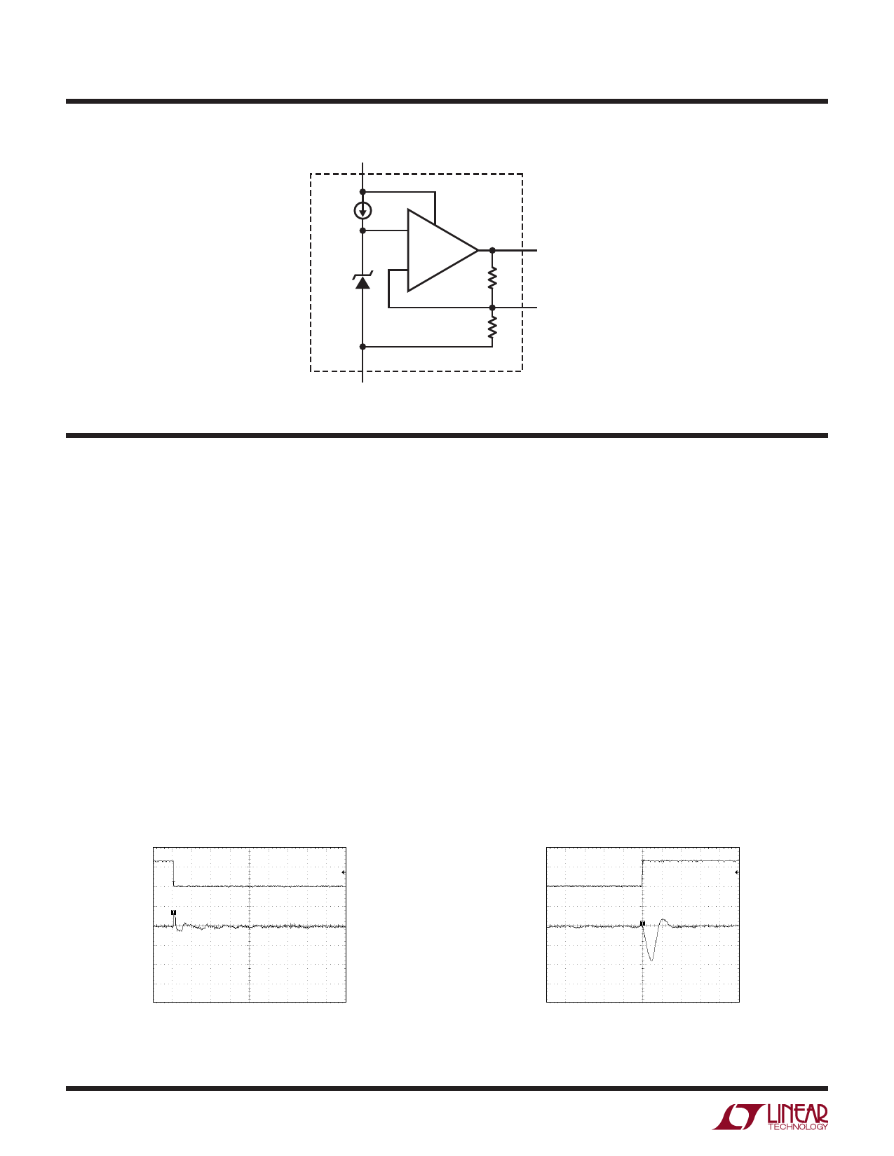
LTC1798 Series
APPLICATIO S I FOR ATIO
Longer Battery Life
Series references have an advantage over shunt style
references. To operate, shunt references require a resistor
between the power supply and the output. This resistor
must be chosen to supply the maximum current that is
demanded by the circuit being regulated. When the circuit
being controlled is not operating at this maximum current,
the shunt reference must always sink this current, result-
ing in high power dissipation and short battery life.
The LTC1798 series low dropout references do not require
a current setting resistor and can operate with any supply
voltage from (VOUT(NOMINAL) + 0.2V) to 12.6V. When the
circuitry being regulated does not demand current, the
LTC1798 series reduces its dissipation and battery life is
extended. If the reference is not delivering load current it
dissipates only 10.8µW when operating on a 2.7V supply
for LTC1798-2.5, yet the same connection can deliver
10mA of load current when demanded.
capacitance is required, a resistor in series with the
capacitor is recommended to reduce the output ringing.
Figure 2 illustrates the use of a damping resistor for
capacitive loads greater than 1µF. Figure 3 shows the
resistor and capacitor values required to achieve critical
damping.
5.2V
TO
12.6V
0.1µF
LTC1798-5
2
IN
6
OUT
GND
4
5V
COUT
>1µF
DAMPING RESISTOR
<1k
1798 F02
Figure 2. Adding a Damping Resistor with
Output Capacitors Greater Than 1µF
10k
Output Bypass Capacitor
The LTC1798 series is designed to be stable with or
without capacitive loads. With no capacitive load, the
reference is ideal for fast settling applications, or where PC
board space is at a premium.
In applications with significant output loading changes,
an output bypass capacitor of up to 1µF can be used to
improve the output transient response. Figure 1 shows
the response of the reference to a 1mA to 0µA load step
with a 1µF output capacitor. If more than 1µF of output
1k
100
10
1
10
100
1000
OUTPUT CAPACITOR VALUE (µF)
1798 F03
Figure 3. Damping Resistance vs Output Capacitor Value
1mA
IOUT
0mA
VOUT
100mV/DIV
1mA
IOUT
0mA
VOUT
100mV/DIV
10ms/DIV
0.5ms/DIV
1798 F01a
1798 F01b
Figure 1. Reference Output Load Transient Response, 1µF Output Capacitor
6
Share Link: 