LV4991TT(2007) データシートの表示(PDF) - SANYO -> Panasonic
部品番号
コンポーネント説明
メーカー
LV4991TT Datasheet PDF : 11 Pages
| |||
LV4991TT
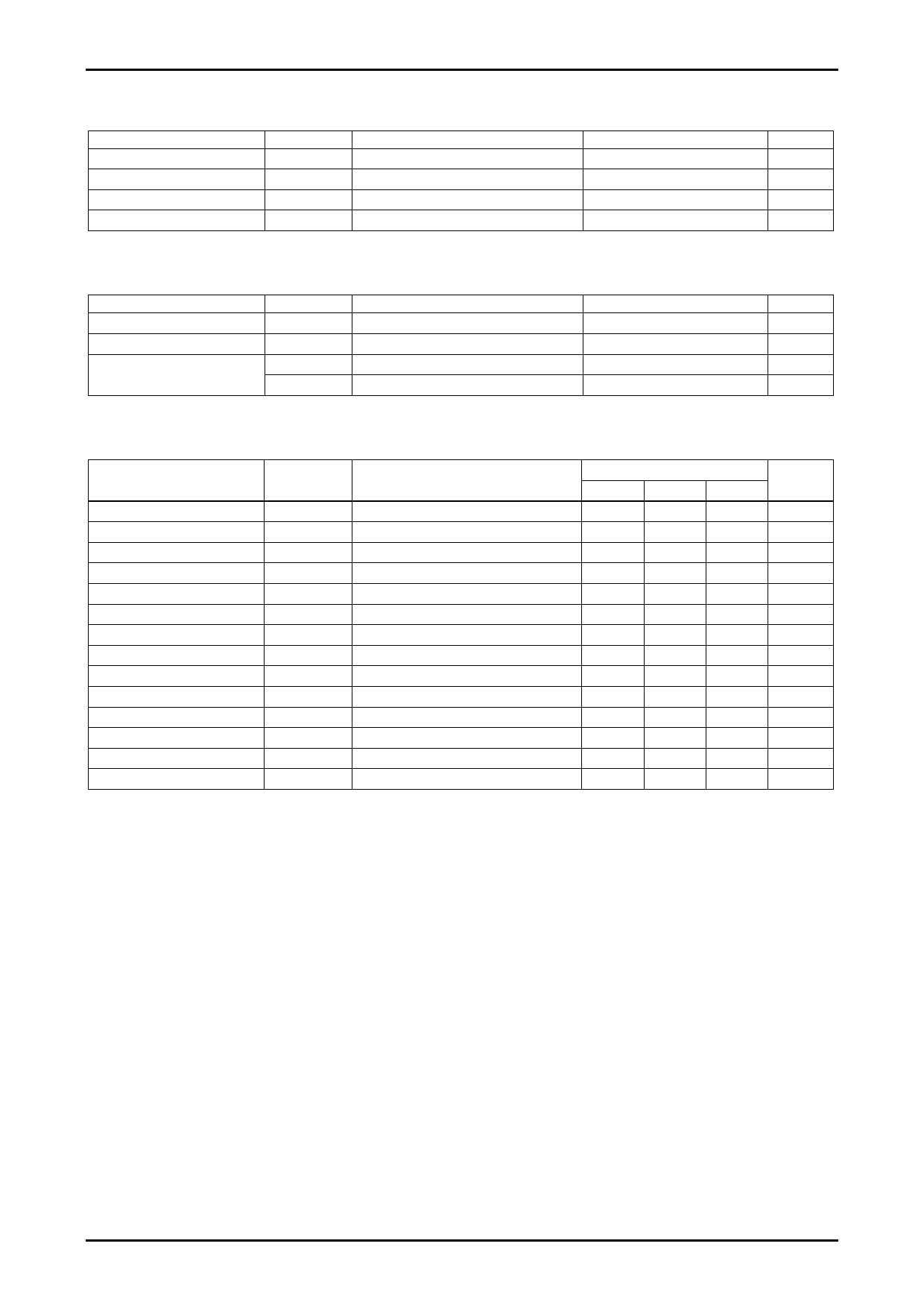
Specifications
Maximum Ratings at Ta = 25°C
Parameter
Maximum supply voltage
Allowable power dissipation
Symbol
VCC max
Pd max
Conditions
Substrate mounted*
Operating temperature
Topr
Storage temperature
Tstg
* Substrate mounted : with 58mm × 89mm × 1.6mm, glass epoxy substrate
Operating Conditions at Ta = 25°C
Parameter
Recommended supply voltage
Recommended load resistance
Allowable operating supply
voltage range
Symbol
VCC
RL
VCC op1
VCC op2
Conditions
(at RL = 8Ω)
(at RL = 16 to 32Ω)
* Determine the supply voltage to be used with due consideration of allowable power dissipation.
Electrical Characteristics Ta = 25°C, VCC = 3.6V, fin = 1kHz, RL = 8Ω
Parameter
Symbol
Conditions
Quiescent current drain
Stand-by current drain
Maximum output power
Voltage gain
Voltage gain use range
Total harmonic distortion ratio
Output noise voltage
Ripple removal ratio
Output offset voltage
Reference (pin 3) voltage
Pin 2 control HIGH voltage
Pin 2 control LOW voltage
Pin 4 control HIGH voltage
Pin 4 control LOW voltage
ICCOP
ISTBY
POMX
VG
VGR
THD
VNOUT
SVRR
VOS
VREF
VSTBH
VSTBL
VCNTH
VCNTL
No signal, RL = ∞
No signal, RL = ∞, V2 = LOW
THD = 10%
VIN = -30dBV
VIN = -30dBV
Rg = 620Ω, 20 to 20kHz
Rg = 620Ω, fr = 100Hz, Vr = -20dBV
Rg = 620Ω
Power amplifier operation mode
Power amplifier standby mode
Second power amplifier operation mode
Second power amplifier standby mode
Ratings
Unit
6
V
750
mV
-40 to +85
°C
-40 to +150
°C
Ratings
Unit
3.6
V
8 to 32
Ω
2.7 to 4.0
V
2.7 to 5.5
V
min
300
4.5
0
-50
1.9
0
1.6
0
Ratings
typ
3.6
0.1
450
6
0.3
120
48
1.81
max
6
10
7.5
26
1
280
50
VCC
0.3
VCC
0.3
Unit
mA
µA
mW
dB
dB
%
µVrms
dB
mV
V
V
V
V
V
No.A0739-2/11
Share Link: 