M29F002 データシートの表示(PDF) - STMicroelectronics
部品番号
コンポーネント説明
メーカー
M29F002 Datasheet PDF : 29 Pages
| |||
M29F002T, M29F002NT, M29F002B
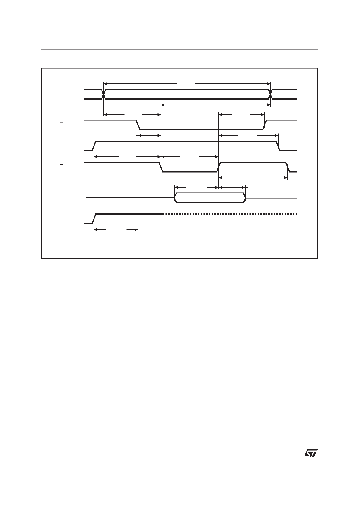
Figure 7. Write AC Waveforms, W Controlled
A0-A17
E
G
W
DQ0-DQ7
tAVWL
tELWL
tGHWL
tAVAV
VALID
tWLAX
tWHEH
tWHGL
tWLWH
tDVWH
VALID
tWHWL
tWHDX
VCC
tVCHEL
AI02083
Note: Address are latched on the falling edge of W, Data is latched on the rising edge of W.
Erase Suspend (ES) Instruction. The Block
Erase operation may be suspended by this instruc-
tion which consists of writing the command B0h
without any specific address. No Coded cycles are
required. It permits reading of data from another
block and programming in another block while an
erase operation is in progress. Erase suspend is
accepted only during the Block Erase instruction
execution. Writing this command during Erase
timeout will, in addition to suspending the erase,
terminate the timeout. The Toggle bit DQ6 stops
togglingwhen the P/E.C. is suspended.The Toggle
bits will stop toggling between 0.1µs and 15µs after
the Erase Suspend (ES) command has been writ-
ten. The device will then automatically be set to
Read Memory Array mode. When erase is sus-
pended, a Read from blocks being erased will
output DQ2 toggling and DQ6 at ’1’. A Read from
a block not being erased returns valid data. During
suspension the memory will respond only to the
Erase Resume ER and the Program PG instruc-
tions. A Program operation can be initiated during
erase suspend in one of the blocks not being
erased. It will result in both DQ2 and DQ6 toggling
when the data is beingprogrammed. ARead/Reset
16/29
command will definitively abort erasure and result
in invalid data in the blocks being erased.
Erase Resume (ER) Instruction. If an Erase Sus-
pend instruction was previously executed, the
erase operation may be resumed by giving the
command 30h, at any address, and without any
Coded cycles.
POWER SUPPLY
Power Up
The memory Command Interface is reset on power
up to Read Array. Either E or W must be tied to VIH
during Power Up to allow maximum security and
the possibility to write a command on the first rising
edge of E and W. Any write cycle initiation is
blocked when Vcc is below VLKO.
Supply Rails
Normal precautions must be taken for supply volt-
age decoupling; each device in a system should
have the VCC rail decoupledwith a 0.1µF capacitor
close to the VCC and VSS pins. The PCB trace
widths should be sufficient to carry the VCC pro-
gram and erase currents required.
Share Link: 