M29F400 データシートの表示(PDF) - STMicroelectronics
部品番号
コンポーネント説明
メーカー
M29F400 Datasheet PDF : 40 Pages
| |||
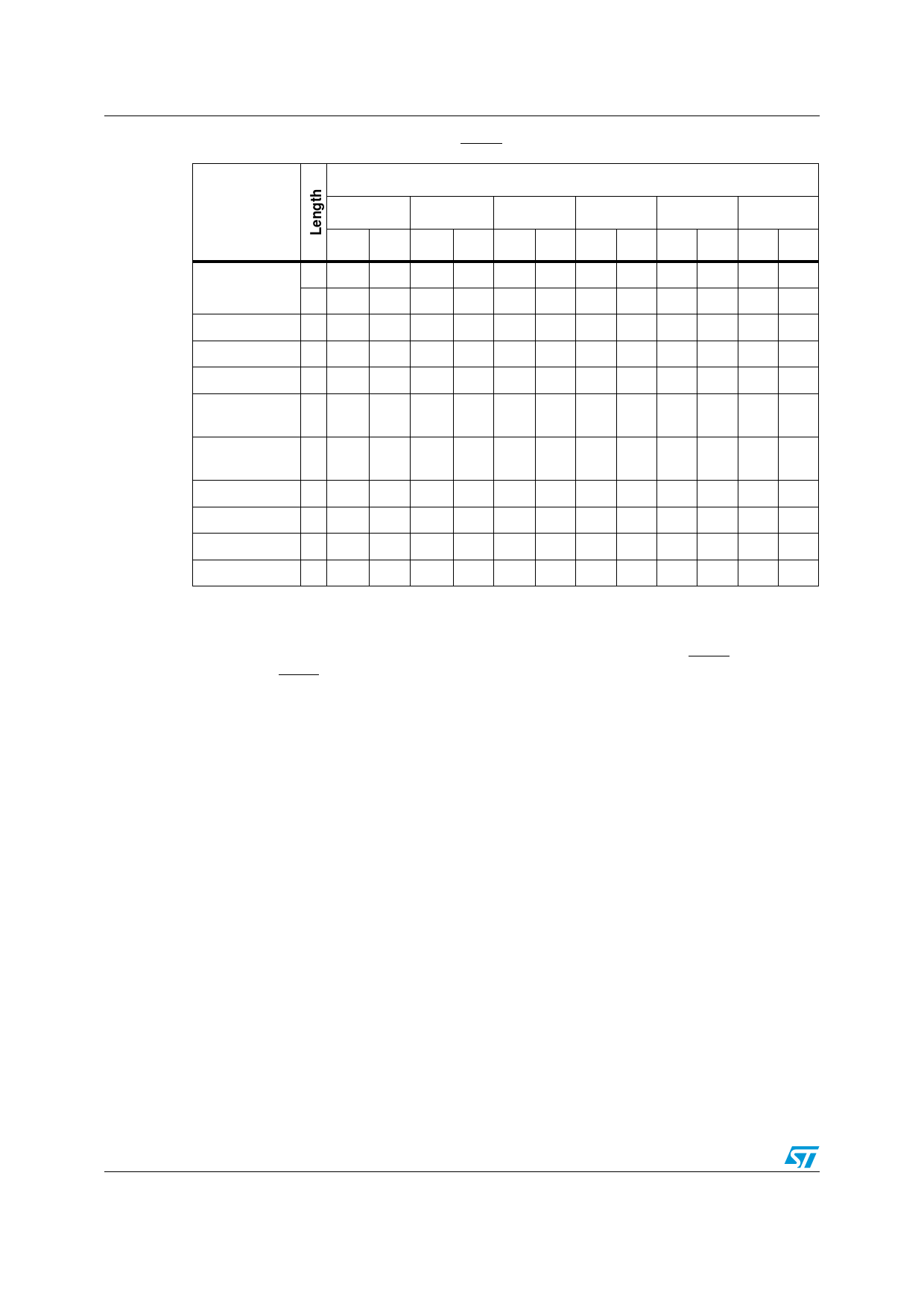
Command interface
M29F400BT, M29F400BB
Table 5.
Commands, 8-bit mode, BYTE = VIL(1) (2)
Bus Write Operations
Command
1st
2nd
3rd
4th
5th
6th
Addr Data Addr Data Addr Data Addr Data Addr Data Addr Data
Read/Reset
1 X F0
3 AAA AA 555 55 X F0
Auto Select
3 AAA AA 555 55 AAA 90
Program
4 AAA AA 555 55 AAA A0 PA PD
Unlock Bypass 3 AAA AA 555 55 AAA 20
Unlock Bypass
Program
2
X
A0 PA PD
Unlock Bypass
Reset
2
X
90
X
00
Chip Erase
6 AAA AA 555 55 AAA 80 AAA AA 555 55 AAA 10
Block Erase
6+ AAA AA 555 55 AAA 80 AAA AA 555 55 BA 30
Erase Suspend 1 X B0
Erase Resume 1 X 30
1. X = Don’t Care, PA = Program Address, PD = Program Data, BA = Any address in the Block.
2. All values are in hexadecimal.
The Command Interface only uses A–1, A0-A10 and DQ0-DQ7 to verify the commands;
A11-A17, DQ8-DQ14 and DQ15 are Don’t Care. DQ15A–1 is A–1 when BYTE is VIL or
DQ15 when BYTE is VIH.
4.11
Read/Reset
After a Read/Reset command, read the memory as normal until another command is
issued.
4.12
Auto Select
After an Auto Select command, read Manufacturer ID, Device ID or Block Protection Status.
4.13
Program, Unlock Bypass Program, Chip Erase, Block Erase
After these commands read the Status Register until the Program/Erase Controller
completes and the memory returns to Read Mode. Add additional Blocks during Block
Erase Command with additional Bus Write Operations until Timeout Bit is set.
20/40
Share Link: 