M50LPW080 データシートの表示(PDF) - STMicroelectronics
部品番号
コンポーネント説明
メーカー
M50LPW080 Datasheet PDF : 44 Pages
| |||
M50LPW080
LOW PIN COUNT (LPC) INTERFACE CONFIGURATION REGISTERS
When the Low Pin Count Interface is selected sev-
eral additional registers can be accessed. These
registers control the protection status of the Blocks
and read the General Purpose Input pins. See Ta-
ble 12. for an example of the Register Configura-
tion map, valid for the boot memory, i.e. ID0-ID1
floating or driven LOW, VIL and A20-A21 set to ‘1’.
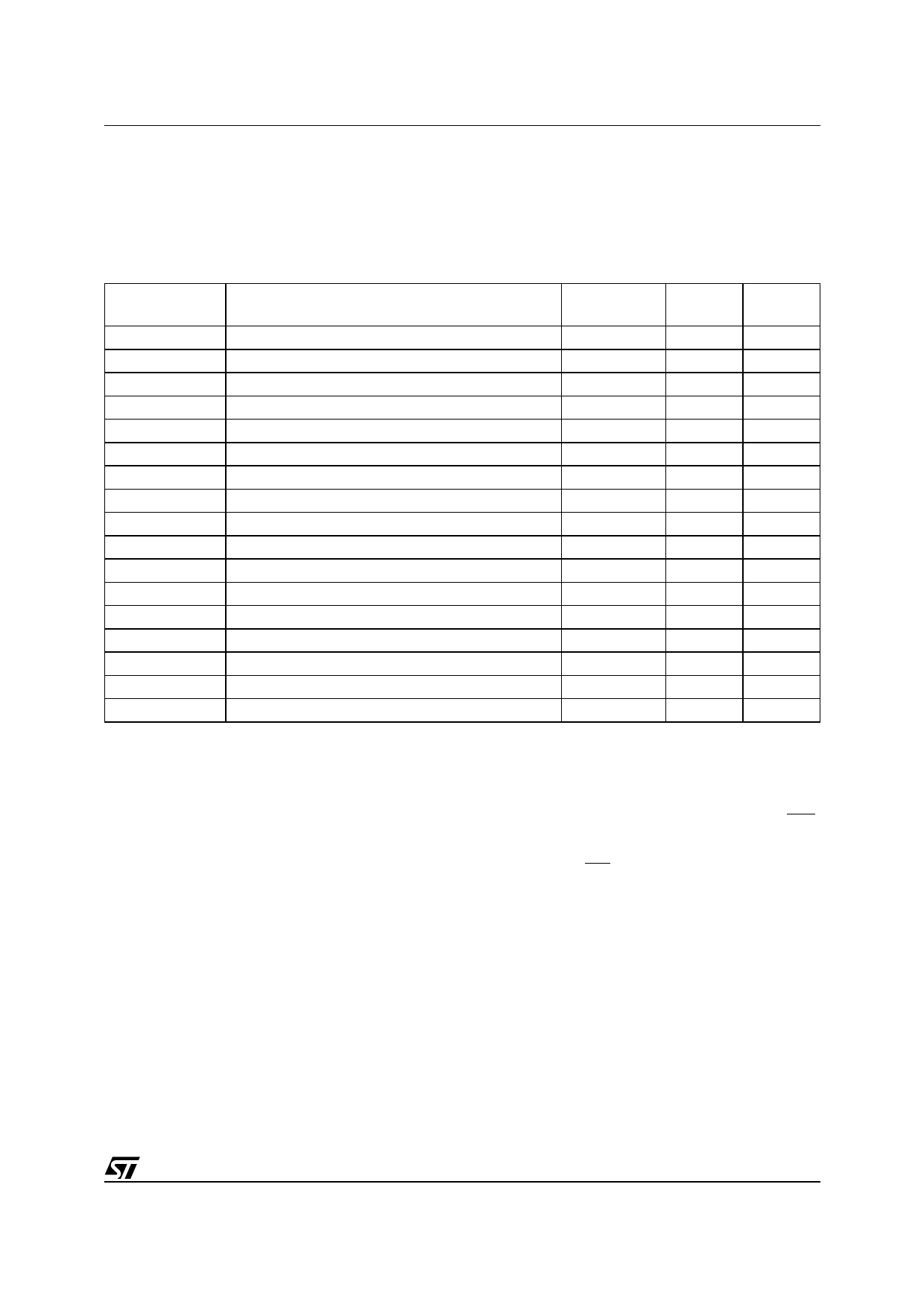
Table 12. Low Pin Count Register Configuration Map (1)
Mnemonic
Register Name
Memory
Address
Default
Value
Access
T_BLOCK_LK Top Block Lock Register (Block 15)
FFBF0002h
01h
R/W
T_MINUS01_LK Top Block [-1] Lock Register (Block 14)
FFBE0002h
01h
R/W
T_MINUS02_LK Top Block [-2] Lock Register (Block 13)
FFBD0002h
01h
R/W
T_MINUS03_LK Top Block [-3] Lock Register (Block 12)
FFBC0002h
01h
R/W
T_MINUS04_LK Top Block [-4] Lock Register (Block 11)
FFBB0002h
01h
R/W
T_MINUS05_LK Top Block [-5] Lock Register (Block 10)
FFBA0002h
01h
R/W
T_MINUS06_LK Top Block [-6] Lock Register (Block 9)
FFB90002h
01h
R/W
T_MINUS07_LK Top Block [-7] Lock Register (Block 8)
FFB80002h
01h
R/W
T_MINUS08_LK Top Block [-8] Lock Register (Block 7)
FFB70002h
01h
R/W
T_MINUS09_LK Top Block [-9] Lock Register (Block 6)
FFB60002h
01h
R/W
T_MINUS10_LK Top Block [-10] Lock Register (Block 5)
FFB50002h
01h
R/W
T_MINUS11_LK Top Block [-11] Lock Register (Block 4)
FFB40002h
01h
R/W
T_MINUS12_LK Top Block [-12] Lock Register (Block 3)
FFB30002h
01h
R/W
T_MINUS13_LK Top Block [-13] Lock Register (Block 2)
FFB20002h
01h
R/W
T_MINUS14_LK Top Block [-14] Lock Register (Block 1)
FFB10002h
01h
R/W
T_MINUS15_LK Top Block [-15] Lock Register (Block 0)
FFB00002h
01h
R/W
GPI_REG
General Purpose Input Register
FFBC0100h
N/A
R
Note: 1. This map is referred to the boot memory (ID0-ID1 floating or driven, LOW, VIL and A20-A21 set to ‘1’).
Lock Registers
through the Lock Register and may be modified
The Lock Registers control the protection status of unless write protected through some other means.
the Blocks. Each Block has its own Lock Register.
Three bits within each Lock Register control the
When VPP is less than VPPLK all blocks are pro-
tected and cannot be modified, regardless of the
protection of each block, the Write Lock Bit, the state of the Write Lock Bit. If Top Block Lock, TBL,
Read Lock Bit and the Lock Down Bit.
The Lock Registers can be read and written,
though care should be taken when writing as, once
the Lock Down Bit is set, ‘1’, further modifications
to the Lock Register cannot be made until cleared,
is Low, VIL, then the Top Block (Block 15) is write
protected and cannot be modified. Similarly, if
Write Protect, WP, is Low, VIL, then the Main
Blocks (Blocks 0 to 14) are write protected and
cannot be modified.
to ‘0’, by a reset or power-up.
After power-up or reset the Write Lock Bit is al-
See Table 13. for details on the bit definitions of ways set to ‘1’ (write protected).
the Lock Registers.
Read Lock. The Read Lock bit determines
Write Lock. The Write Lock Bit determines
whether the contents of the Block can be modified
(using the Program or Block Erase Command).
When the Write Lock Bit is set, ‘1’, the block is
write protected; any operations that attempt to
change the data in the block will fail and the Status
Register will report the error. When the Write Lock
whether the contents of the Block can be read
(from Read mode). When the Read Lock Bit is set,
‘1’, the block is read protected; any operation that
attempts to read the contents of the block will read
00h instead. When the Read Lock Bit is reset, ‘0’,
read operations in the Block return the data pro-
grammed into the block as expected.
Bit is reset, ‘0’, the block is not write protected After power-up or reset the Read Lock Bit is al-
ways reset to ‘0’ (not read protected).
21/44
Share Link: 