M58BV016DB7T3F データシートの表示(PDF) - Micron Technology
部品番号
コンポーネント説明
メーカー
M58BV016DB7T3F Datasheet PDF : 70 Pages
| |||
M58BW016DT, M58BW016DB, M58BW016FT, M58BW016FB
Bus operations
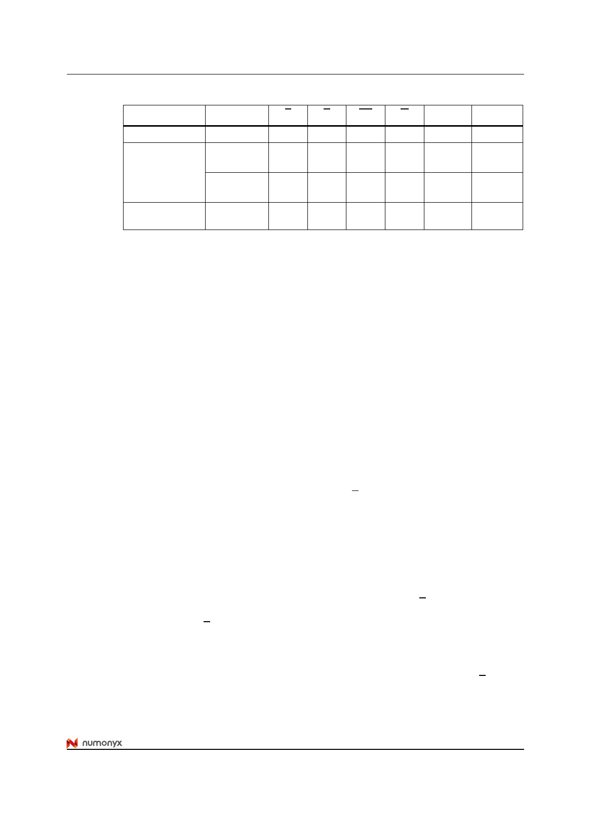
Table 5. Asynchronous read electronic signature operation
Code
Device
E
G
GD
W
Manufacturer
All
VIL
VIL
VIH
VIH
Device
M58BW016DT
M58BW016FT VIL
VIL
VIH
VIH
M58BW016DB
M58BW016FB VIL
VIL
VIH
VIH
Burst configuration
register
VIL
VIL
VIH
VIH
1. BCR = Burst configuration register.
A18-A0 DQ31-DQ0
00000h 00000020h
00001h 00008836h
00001h 00008835h
00005h
BCR(1)
3.2
Synchronous bus operations
For synchronous bus operations refer to Table 6 together with the following text.
3.2.1
Caution:
Synchronous burst read
Synchronous burst read operations are used to read from the memory at specific times
synchronized to an external reference clock.
In the M58BW016FT and M58BW016FB only, once the memory is configured in burst
mode, it is mandatory to have an active clock signal since the switching of the output buffer
data bus is synchronized to the active edge of the clock. In the absence of clock, no data is
output.
The M58BW016DT and M58BW016DB are not concerned by the paragraph above.
The burst type, length and latency can be configured. The different configurations for
synchronous burst read operations are described in Section 3.3: Burst configuration
register. Refer to Figure 4 and Figure 5 for examples of synchronous burst operations.
In continuous burst read, one burst read operation can access the entire memory
sequentially by keeping the Burst Address Advance B at VIL for the appropriate number of
clock cycles. At the end of the memory address space the burst read restarts from the
beginning at address 000000h.
A valid synchronous burst read operation begins when the Burst Clock is active and Chip
Enable and Latch Enable are Low, VIL. The burst start address is latched and loaded into
the internal burst address counter on the valid Burst Clock K edge (rising or falling
depending on the value of M6) or on the rising edge of Latch Enable, whichever occurs first.
After an initial memory latency time, the memory outputs data each clock cycle (or two clock
cycles depending on the value of M9). The Burst Address Advance B input controls the
memory burst output. The second burst output is on the next clock valid edge after the Burst
Address Advance B has been pulled Low.
Valid Data Ready, R, monitors if the memory burst boundary is exceeded and the burst
controller of the microprocessor needs to insert wait states. When Valid Data Ready is Low
on the active clock edge, no new data is available and the memory does not increment the
internal address counter at the active clock edge even if Burst Address Advance, B, is Low.
21/70
Share Link: 