M58MR064D データシートの表示(PDF) - STMicroelectronics
部品番号
コンポーネント説明
メーカー
M58MR064D Datasheet PDF : 52 Pages
| |||
M58MR064C, M58MR064D
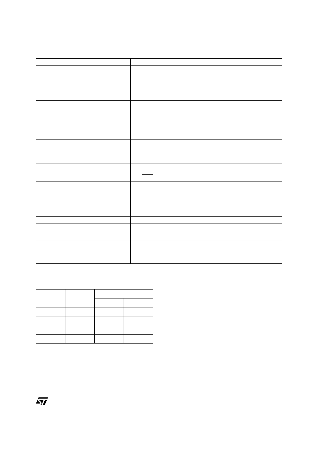
Table 14. Read Configuration Register (AS and Read CFI instructions) (1)
Configuration Register
Function
CR15
Read mode
0 = Synchronous Burst mode read
1 = Asynchronous Page mode read (default)
CR14
Bus Invert configuration (power save)
0 = disabled (default)
1 = enabled
CR13-CR11
X-Latency
010 = 2 clock latency
011 = 3 clock latency
100 = 4 clock latency
101 = 5 clock latency
111 = reserved
Other configurations reserved
CR10
Power-down configuration
0 = power-down disabled (default)
1 = power-down enabled
CR9
Reserved
CR8
Wait configuration
0 = WAIT is active during wait state
1 = WAIT is active one data cycle before wait state (default)
CR7
Burst order configuration
0 = Interleaved
1 = Linear (default)
CR6
Clock configuration
0 = Address latched and data output on the falling clock edge
1 = Address latched and data output on the rising clock edge (default)
CR5-CR4
Reserved
CR3
Burst Wrap
0 = burst wrap within burst length set by CR2-CR0
1 = Don’t wrap accesses within burst length set by CR2-CR0 (default)
CR2-CR0
Burst length
001 = 4 word burst length
010 = 8 word burst length
111 = Continuous burst mode (requires CR7 = 1)
Note: 1. The RCR can be read via the RSIG command (90h). Bank A Address + 05h contains the RCR data. See Table 9.
2. All the bits in the RCR are set to default on device power-up or reset.
Table 15. BINV Configuration Bits
CR15
CR14
BINV
IN
OUT
0
0
X
0
0
1
Active
Active
1
0
X
0
1
1
Active
0
19/52
Share Link: 