M59DR032EA データシートの表示(PDF) - STMicroelectronics
部品番号
コンポーネント説明
メーカー
M59DR032EA Datasheet PDF : 43 Pages
| |||
M59DR032EA, M59DR032EB
s The fourth latches the Address and the Data to
be written to the Protection Register and starts
the Program/Erase Controller.
Read operations output the Status Register con-
tent after the programming has started.
The OTP segment can be protected by program-
ming bit 1 of the Protection Register Lock. The
segment can be protected by programming bit 1 of
the Protection Register Lock. Bit 1 of the Protec-
tion Register Lock also protects bit 2 of the Protec-
tion Register Lock. Programming bit 2 of the
Protection Register Lock will result in a permanent
protection of Parameter Block #0 (see Figure 4,
Security Block and Protection Register Memory
Map). Attempting to program a previously protect-
ed Protection Register will result in a Status Reg-
ister error. The protection of the Protection
Register and/or the Security Block is not revers-
ible.
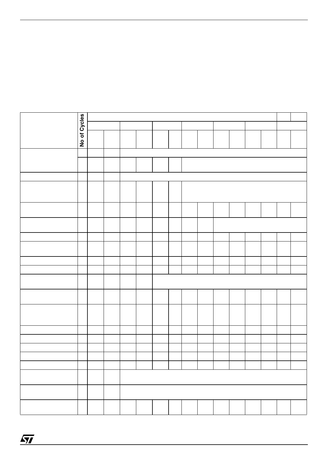
Table 4. Commands
Commands
Bus Operations
1st
2nd
3rd
4th
5th
6th
7th
Add
Data
Add
Data
Add
Dat
a
Add
Data
Add
Data
Add
Data Add Data
Read/Reset
1+ X F0h
Read Memory Array until a new write cycle is initiated.
3+ 555h AAh 2AAh 55h 555h F0h
Read Memory Array until a new write cycle is
initiated.
CFI Query
1+ 55h 98h Read CFI and Electronic Signature until a Read/Reset command is issued.
Auto Select
Read Protection Register, Block Protection or
3+ 555h AAh 2AAh 55h 555h 90h Configuration Register Status until a Read/Reset
command is issued.
Set Configuration
Register
4 555h AAh 2AAh 55h 555h 60h CRD 03h
Program
4 555h AAh 2AAh 55h 555h A0h PA
PD
Read Data Polling or Toggle Bit until
Program completes.
Double Word Program 5 555h AAh 2AAh 55h 555h 40h PA1 PD1 PA2 PD2
Quadruple Word
Program
5 555h AAh 2AAh 55h 555h 50h PA1 PD1 PA2 PD2 PA3 PD3 PA4 PD4
Enter Bypass Mode 3 555h AAh 2AAh 55h 555h 20h
Exit Bypass Mode
2 X 90h X 00h
Program in Bypass
Mode
2 X A0h PA PD
Read Data Polling or Toggle Bit until Program completes.
Double Word Program
in Bypass Mode
3
X
40h PA1 PD1 PA2 PD2
Quadruple Word
Program in Bypass
Mode
3 X 50h PA1 PD1 PA2 PD2 PA3 PD3 PA4 PD4
Block Lock
4 555h AAh 2AAh 55h 555h 60h BA 01h
Block Unlock
4 555h AAh 2AAh 55h 555h 60h BA D0h
Block Lock-Down
4 555h AAh 2AAh 55h 555h 60h BA 2Fh
Block Erase
6+ 555h AAh 2AAh 55h 555h 80h 555h AAh 2AAh 55h BA 30h
Bank Erase
6 555h AAh 2AAh 55h 555h 80h 555h AAh 2AAh 55h BA 10h
Erase Suspend
1
X
B0h
Read until Toggle stops, then read all the data needed from any Blocks not
being erased then Resume Erase.
Erase Resume
1 BA 30h
Read Data Polling or Toggle Bits until Erase completes or Erase is
suspended another time
Protection Register
Program
4 555h AAh 2AAh 55h PA C0h PA PD
Note: X = Don’t Care, BA = Block Address, PA = Program address, PD = Program Data, CRD = Configuration Register Data. For Coded
cycles address inputs A12-A20 are don’t care.
13/43
Share Link: 