98ASB42345B データシートの表示(PDF) - Freescale Semiconductor
部品番号
コンポーネント説明
メーカー
98ASB42345B Datasheet PDF : 38 Pages
| |||
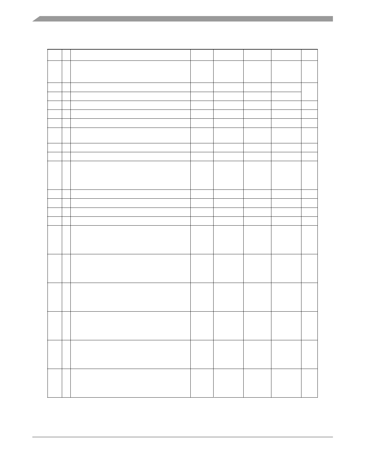
Electrical Characteristics
Table 7. DC Characteristics (continued)
Num C
Parameter
Symbol Min
Typical1
Max Unit
Output low current — Max total IOL for all ports
5P
5 V IOLT
—
3V
—
6 P Input high voltage; all digital inputs
VIH 0.65 × VDD
7 P Input low voltage; all digital inputs
VIL
—
8 P Input hysteresis; all digital inputs
9 C Input leakage current; input only pins2
10 P High impedance (off-state) leakage current2
Vhys
|IIn|
|IOZ|
0.06 × VDD
—
—
11
C
Total leakage combined for all inputs and Hi-Z pins
— All input only and I/O2
|IOZTOT|
—
12 P Internal pullup resistors3
RPU
13 P Internal pulldown resistors4
RPD
DC injection current 5, 6, 7
14
D
VIN < VSS, VIN > VDD
Single pin limit
IIC
Total MCU limit, includes sum of all stressed pins
20
20
–0.2
–5
15 C Input capacitance; all non-supply pins
CIn
—
16 C RAM retention voltage
17 P POR re-arm voltage8
VRAM
0.6
VPOR
0.9
18 D POR re-arm time
tPOR
10
Low-voltage detection threshold —
19 P high range
VDD falling VLVD1
3.9
VDD rising
4.0
Low-voltage detection threshold —
20 P low range
VDD falling VLVD0
VDD rising
2.48
2.54
Low-voltage warning threshold —
21 C high range 1
VDD falling VLVW3
4.5
VDD rising
4.6
Low-voltage warning threshold —
22 P high range 0
VDD falling VLVW2
4.2
VDD rising
4.3
Low-voltage warning threshold
23 P low range 1
VDD falling VLVW1
VDD rising
2.84
2.90
Low-voltage warning threshold —
24 C low range 0
VDD falling VLVW0
VDD rising
2.66
2.72
—
—
—
—
—
0.1
0.1
—
45
45
—
—
—
1.0
1.4
—
4.0
4.1
2.56
2.62
4.6
4.7
4.3
4.4
2.92
2.98
2.74
2.80
100
mA
60
—
V
0.35 × VDD
—
mV
1
μA
1
μA
2
μA
65
kΩ
65
kΩ
0.2
mA
5
8
pF
—
V
2.0
V
—
μs
4.1
V
4.2
2.64
V
2.70
4.7
V
4.8
4.4
V
4.5
3.00
V
3.06
2.82
V
2.88
MC9S08SE8 Series MCU Data Sheet, Rev. 3
10
Freescale Semiconductor
Share Link: 