ISPLSI5384VA-70LQ208I データシートの表示(PDF) - Lattice Semiconductor
部品番号
コンポーネント説明
メーカー
ISPLSI5384VA-70LQ208I Datasheet PDF : 31 Pages
| |||
Specifications ispLSI 5384VA
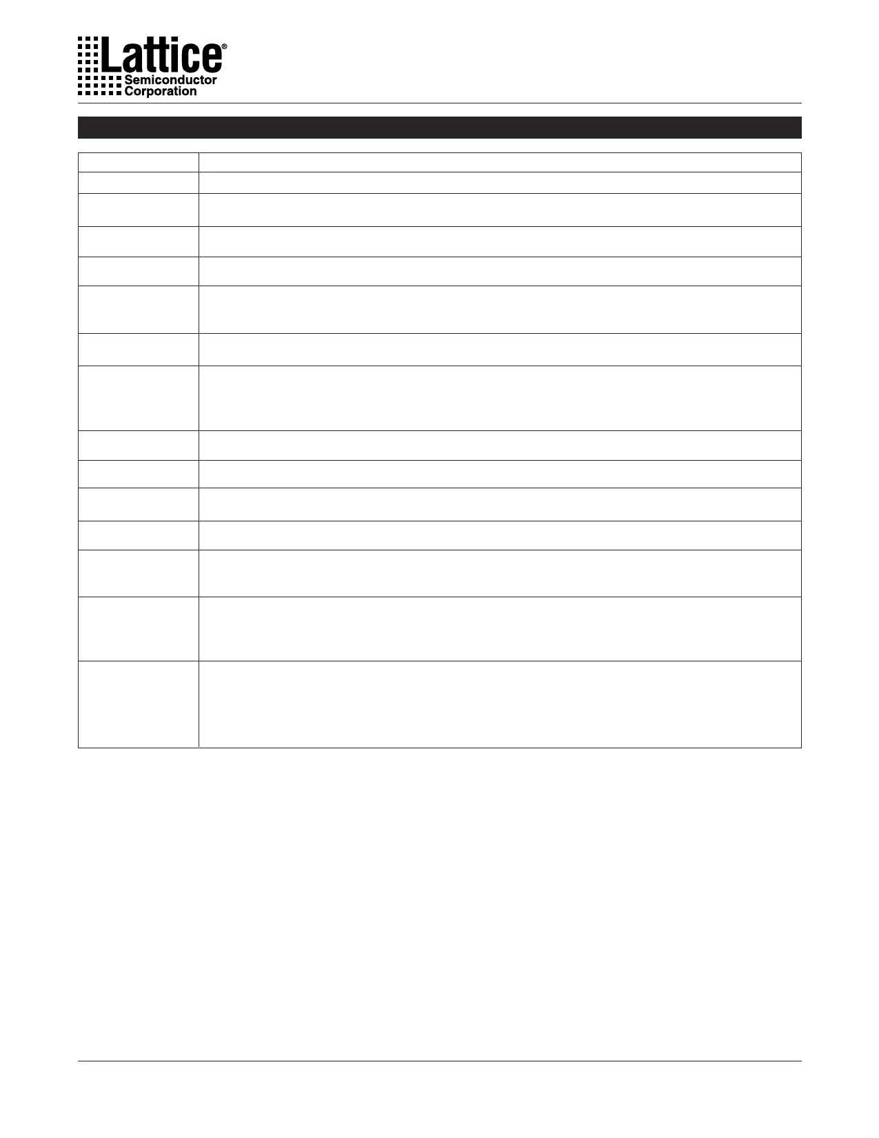
Signal Descriptions
Signal Name
TMS
TCK
TDI
TDO
TOE / I/O0
GOE0, GOE1
GSET/GRST
I/O
GND
NC1
VCC
CLK0, CLK1
CLK2 / I/O,
CLK3 / I/O
VCCIO
Description
Input - This pin is the Test Mode Select input, which is used to control the JTAG state machine.
Input - This pin is the Test Clock input pin used to clock through the JTAG state machine.
Input - This pin is the JTAG Test Data In pin used to load data.
Output - This pin is the JTAG Test Data Out pin used to shift data out.
Input/Output - This pin functions as either the Test Output Enable pin or an I/O pin based upon
customer's design. TOE tristates all I/O pins when a logic low is driven.
Input - These two pins are the Global Output Enable input pins.
Dedicated Set/Reset Input - This pin is available to all registers in the device and can
independently be configured as preset, reset or no effect on each register. The global polarity
(active high or low input) for this pin is also selectable.
Input/Output – These are the general purpose I/O used by the logic array.
Ground
No connect.
Vcc
Dedicated clock inputs for all registers. Both clocks are muxed before being used as the clock
input to all registers in the device.
Input/Output - These pins function as either dedicated clock inputs for all registers or an I/O
pin based upon customer's design. Both clocks are muxed before being used as the clock input
to all registers in the device.
Input - This pin is used if an optional 2.5V output is to be used. Every IO can independently
select either 3.3V or the optional voltage as its output level. If the optional output voltage is
not required, this pin must be connected to the Vcc supply. Programmable pull-up resistors and
bus-hold latches only draw current from this supply.
1. NC pins are not to be connected to any active signals, VCC or GND.
17
Share Link: 