SA9024 データシートの表示(PDF) - Philips Electronics
部品番号
コンポーネント説明
メーカー
SA9024 Datasheet PDF : 23 Pages
| |||
Philips Semiconductors
900 MHz transmit modulator and 1.3 GHz
fractional–N synthesizer
Objective specification
SA9024
REFERENCE R
MAIN M
VCO CYCLES
N
N
N+1
N
N+1
DETECTOR
OUTPUT
ACCUMULATOR
CONTENTS
2
4
1
3
0
FRACTIONAL
COMPENSATION
CURRENT
PULSE
WIDTH
MODULATION
mA
OUTPUT ON
PHP, PHI
µA
PULSE LEVEL
MODULATION
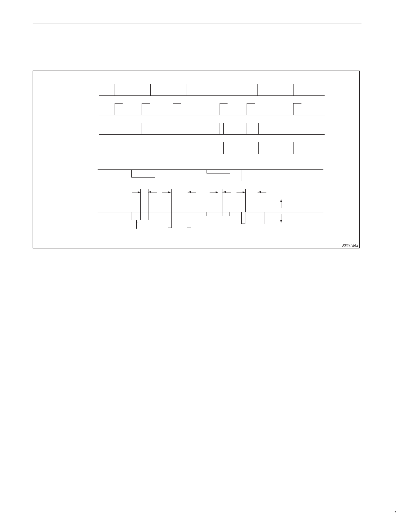
Figure 10. Waveforms for NF = 2; Fraction = 0.4
SR01454
Figure 10 shows that for a proper fractional compensation, the area
of the fractional compensation current pulse must be equal to the
area of the charge pump ripple output.
The fractional compensation current is derived from the main charge
pump in that it will follow all the current scaling through external
resistor setting, programming or speedup operation.
For a given pump,
|comp +
|pump
128
x
Fdac
5 x 128
x
FRD
Where:
Icomp is the compensation current, Ipump is the pump current, Fdac
is the fractional DAC value and FRD is the fractional accumulator
value.
The theoretical value for Fdac would then be: 128 for Fmod = 1
(modulo 5) and 80 for Fmod = 0 (modulo 8).
When the serial input A word is loaded, the output circuits are in the
“speedup mode” as long as the STROBE is H, otherwise the
“normal mode” is active.
Lock Detect
The output LOCK maintains a logic ‘1’ when the auxiliary phase
detector ANDed with the main phase detector ANDed with Offset
Phase Detector indicates a lock condition. During the Standby
mode of operation when the offset loop is unlocked, (SYNEN = low –
see figure 6), the offset phase detector lock output is forced to an on
(locked) state so that the lock detect will give an indication of
receiver lock. The lock condition for the main and auxiliary
synthesizers is defined as a phase difference of less than "1 cycle
on the reference input INR. The LOCK condition is also fulfilled
when the relative counter is disabled (PD1 = ‘0’ or PD2 = ‘0’) for the
main or auxiliary counter, respectively.
Functional Description of Offset Loop, Modulator
and Power Control
Transmit Offset Synthesizer
The transmit offset phase locked loop portion of the SA9024 design
consists of the following functional blocks: reference oscillator,
limiters, phase detector, ÷M, IF VCO and passive loop filter.
Harmonic contents of this signal are attenuated by an LP filter. The
output of the IF VCO is also divided by N and compared with the
reference oscillator in the phase detector.
Reference Oscillator
This Oscillator is used to generate the reference frequency together
with an external crystal and varicap. The output is internally routed
to three buffers and a phase comparator. It is possible to run the
oscillator as an amplifier from an external reference signal (TCXO).
Phase Detector and Charge Pump
The phase comparator is used to compare the output of the divider
with the reference. It provides an output proportional to the phase
difference between the divided down VCO and the reference. This
output is then filtered and used as the control voltage input to the
VCO. The phase detector is a Gilbert multiplier cell type, having a
linear output from 0 to π (π/2 ±π/2), followed by a charge pump. The
charge pump peak output current is programmable to 6.4mA via the
use of an external resistor.
A preliminary design analysis has been performed with the following
loop parameters:
1997 Aug 01
20
Share Link: 