SA9025 データシートの表示(PDF) - Philips Electronics
部品番号
コンポーネント説明
メーカー
SA9025 Datasheet PDF : 23 Pages
| |||
Philips Semiconductors
900 MHz transmit modulator and 2.2 GHz
fractional–N synthesizer
Objective specification
SA9025
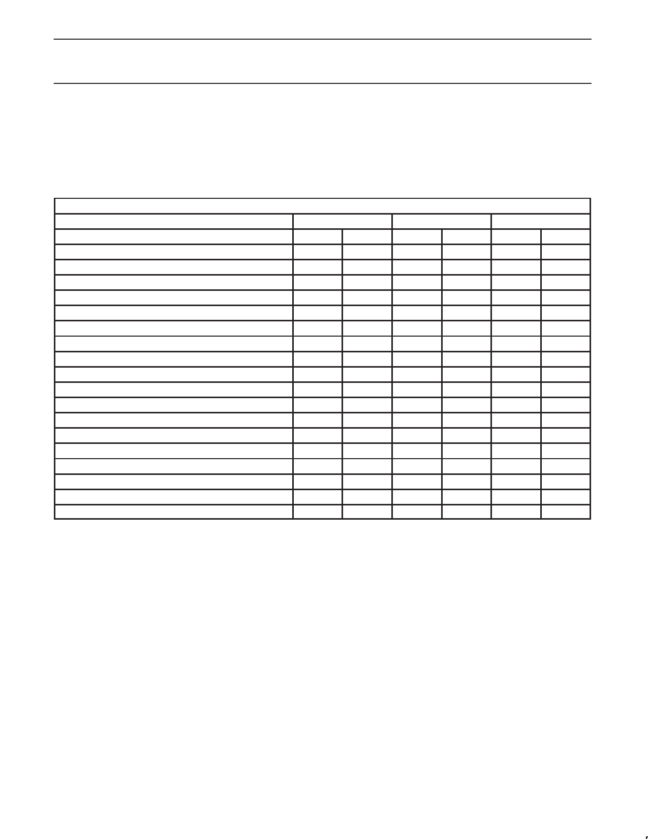
OPERATING MODES & POWER DOWN CONTROL
There are two power saving modes of operation which the SA9025
can be put into, dependent on the status of the system. The
intention of these different modes is to disable circuity that is not in
use at the time in order to reduce power consumption. During sleep
mode, only circuitry which is required to provide a master clock to
the digital portion of the system is enabled. During receive mode,
circuitry which is used to perform the receive function and provide a
master clock is enabled. In transmit mode all the functions of the
chip are enabled which are required to perform transmit, receive and
provide master clock.
SA9025 POWER MODE TRUTH TABLE
Sleep Mode
Enabled
yes
no
Crystal Oscillator
Phase detector and charge pump (transmit offset)
VCO
SSB Up-converter
MCLK Buffer
RCLK Buffer
÷M offset loop divider
TXLO Buffer
RXLO Buffer
I/Q Modulator
Variable Gain Amp.
Control Logic
Main Divider
Reference Divider
Auxiliary Divider
Main Phase Detector and charge pump
Auxiliary Phase Detector and charge pump
Lock Detect
Receive Mode
yes
no
Transmit Mode
yes
no
1997 Aug 01
5
Share Link: 