RC2951(1997) データシートの表示(PDF) - Fairchild Semiconductor
部品番号
コンポーネント説明
メーカー
RC2951 Datasheet PDF : 12 Pages
| |||
RC2951
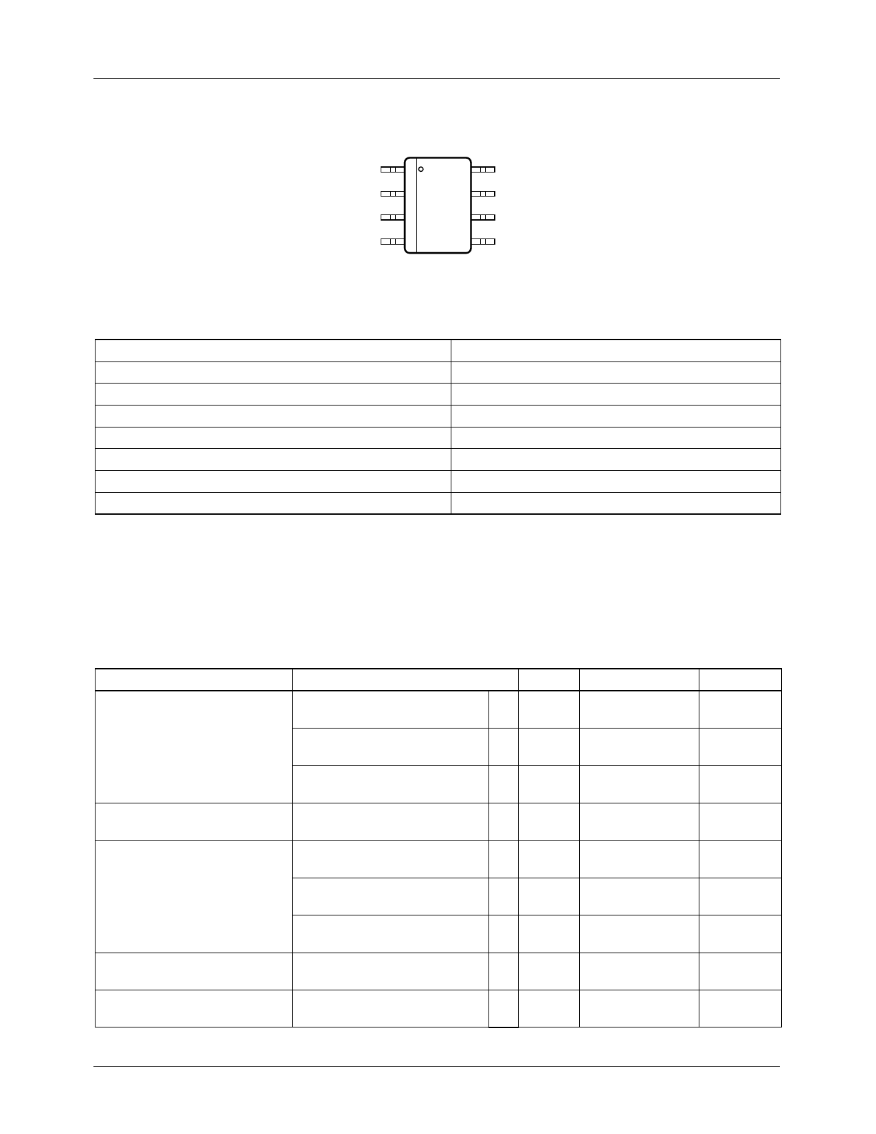
Pin Assignments
8 Lead SOIC Package
PRODUCT SPECIFICATION
Output
1
Sense
2
Shutdown
3
Ground
4
8
Input
7
Feedback
6
VTAP
5
Error
Top View
Absolute Maximum Ratings
Power Dissipation
Lead Temp. (Soldering, 5 seconds)
Storage Temperature Range
Operating Junction Temperature Range1
Input Supply/Voltage
Feedback Input Voltage2,3
Shutdown Input Voltage2
Error Comparator Output Voltage2
Internally Limited
260°C
–65° to +150°C
–55° to +150°C
–0.3 to +30V
–1.5 to +30V
–0.3 to +30V
–0.3 to +30V
Notes:
1. Junction to ambient thermal resistance for the S.O. (M) package is 160°C/W.
2 May exceed input supply voltage.
3. When used in dual-supply systems where the output terminal sees loads returned to a negative supply, the output voltage
should be diode-clamped to ground.
Electrical Characteristics
The • denotes that the limits apply at temperature extremes.
Parameter
Conditions1
Output Voltage
(RC2951M)
TJ = 25°C
-25°C ≤ TJ ≤ 85°C
Output Voltage
(RC2951M)
Output Voltage
(RC2951M-3.3)
Full Operating Temperature
Range
100µA ≤ IL ≤ 100mA
TJ ≤ TJMAX
TJ = 25°C
-25°C ≤ TJ ≤ 85°C
Output Voltage
(RC2951M-3.3)
Output Voltage Temperature
Coefficient7
Full Operating Temperature
Range
100µA ≤ IL ≤ 100mA
TJ ≤ TJMAX
Typ.
5.0
5.0
• 5.0
•
• 5.0
•
3.3
3.3
• 3.3
•
• 3.3
•
• 20
Tested Limit2
5.025
4.975
5.06
4.94
5.075
4.925
3.317
3.284
3.340
3.260
3.346
3.254
120
Units
V max
V min
V max
V min
V max
V min
V max
V min
V max
V min
V max
V min
V max
V min
V max
V min
ppm/°C
2
Share Link: 