HA12229F データシートの表示(PDF) - Hitachi -> Renesas Electronics
部品番号
コンポーネント説明
メーカー
HA12229F
Hitachi -> Renesas Electronics

HA12229F Datasheet PDF : 51 Pages
| |||
HA12228F/HA12229F
Functional Description
Power Supply Range
HA12228F/HA12229F are provided with three line output level, which will permit on optimum overload
margin for power supply conditions. And these are designed to operate on single supply only.
Table 1 Supply Voltage Range
Product
Single Supply
HA12228F
6.5 V to 12.0 V
HA12229F
Note: The lower limit of supply voltage depends on the line output reference level.
The minimum value of the overload margin is specified as 12 dB by Dolby Laboratories.
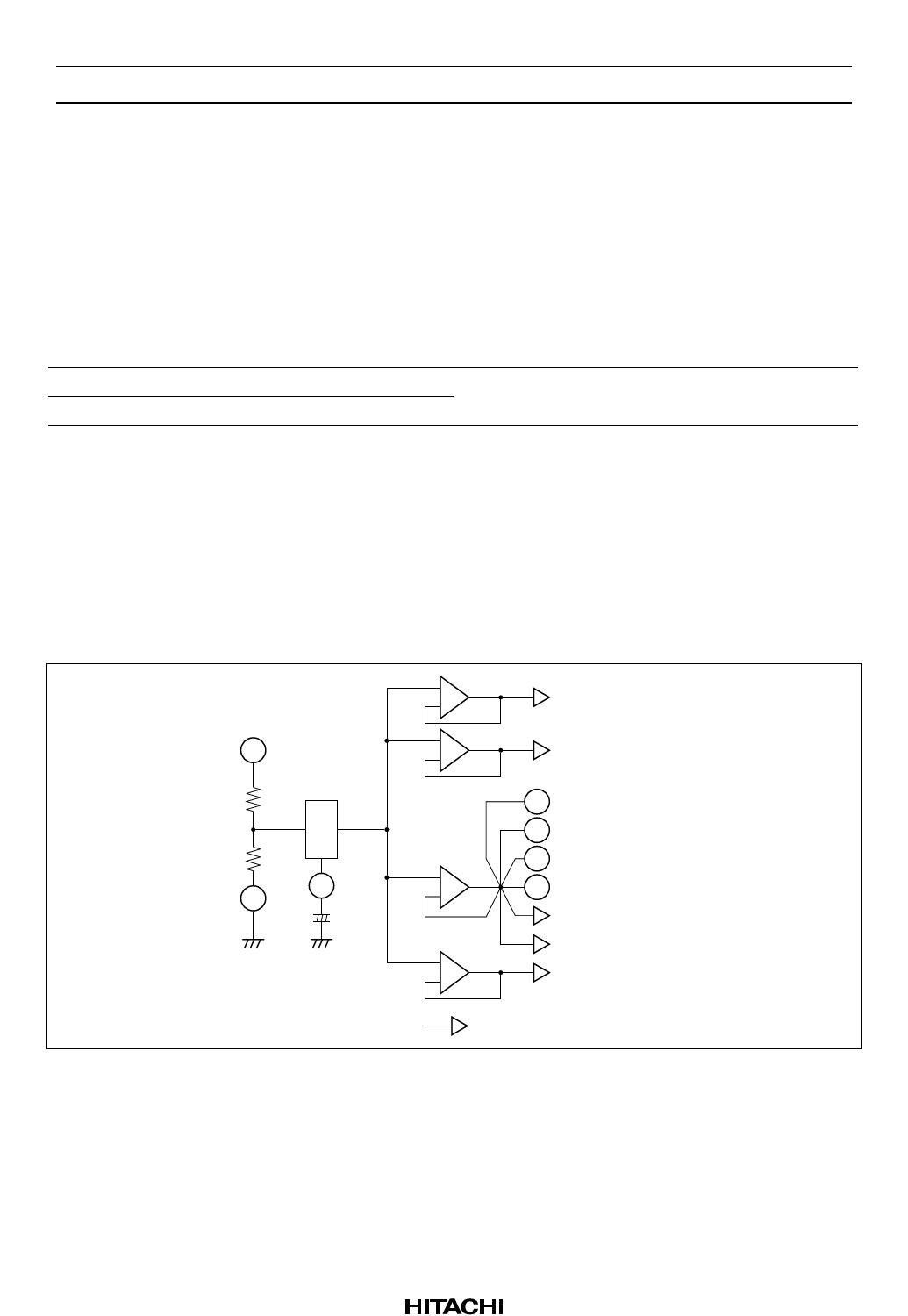
Reference Voltage
These devices provide the reference voltage of half the supply voltage that is the signal grounds. As the
peculiarity of these devices, the capacitor for the ripple filter is very small about 1/100 compared with their
usual value. The block diagram is shown as figure 1.
+
Rch
−
Dolby NR circuit
VCC
15
+
Lch
−
Dolby NR circuit
26
36
+
GND
3 Vref4
28 Vref3
38 Vref2
+
−
32 Vref1
Lch equalizer
Rch equalizer
+
−
MS block
: Internal reference voltage
Figure 1a The HA12228F Block Diagram of Reference Supply Voltage
Rev.2, Dec. 2000, page 9 of 51
Share Link: