TC7106 データシートの表示(PDF) - TelCom Semiconductor Inc => Microchip
部品番号
コンポーネント説明
メーカー
TC7106 Datasheet PDF : 19 Pages
| |||
3-1/2 DIGIT A/D CONVERTERS
1 TC7106
TC7106A
TC7107
TC7107A
Analog Common (Pin 32)
The analog common pin is set at a voltage potential
approximately 3.0V below V+. The potential is guaranteed
to be between 2.7V and 3.35 V below V+. Analog common
is tied internally to the N channel FET capable of sinking
20mA. This FET will hold the common line at 3.0V should an
external load attempt to pull the common line toward V+.
Analog common source current is limited to 10µA. Analog
common is therefore easily pulled to a more negative
voltage (i.e., below V+ – 3.0V).
The TC7106A connects the internal VI+N and VI–N inputs
to analog common during the auto-zero cycle. During the
reference-integrate phase, VI–N is connected to analog com-
mon. If VI–N is not externally connected to analog common,
a common-mode voltage exists. This is rejected by the
converter's 86dB common-mode rejection ratio. In battery
operation, analog common and VI–N are usually connected,
removing common-mode voltage concerns. In systems where
VI–N is connected to the power supply ground or to a given
voltage, analog common should be connected to VI–N.
The analog common pin serves to set the analog section
reference or common point. The TC7106A is specifically
designed to operate from a battery or in any measurement
system where input signals are not referenced (float) with
respect to the TC7106A power source. The analog common
potential of V+ – 3.0V gives a 6 V end of battery life voltage.
The common potential has a 0.001%/% voltage coefficient
and a 15 Ω output impedance.
With sufficiently high total supply voltage (V+ – V–
> 7.0V) analog common is a very stable potential with
excellent temperature stability—typically 20ppm/°C. This
potential can be used to generate the reference voltage. An
external voltage reference will be unnecessary in most
cases because of the 50ppm/°C maximum temperature
coefficient. See Internal Voltage Reference discussion.
Test (Pin 37)
The TEST pin potential is 5V less than V+. TEST may be
used as the negative power supply connection for external
CMOS logic. The TEST pin is tied to the internally generated
negative logic supply (Internal Logic Ground) through a
500Ω resistor in the TC7106A. The TEST pin load should be
no more than 1mA .
If TEST is pulled to V+ all segments plus the minus sign
will be activated. Do not operate in this mode for more than
several minutes with the TC7106A. With TEST = V+ the LCD
segments are impressed with a DC voltage which will
destroy the LCD.
The TEST pin will sink about 10mA when pulled to V+.
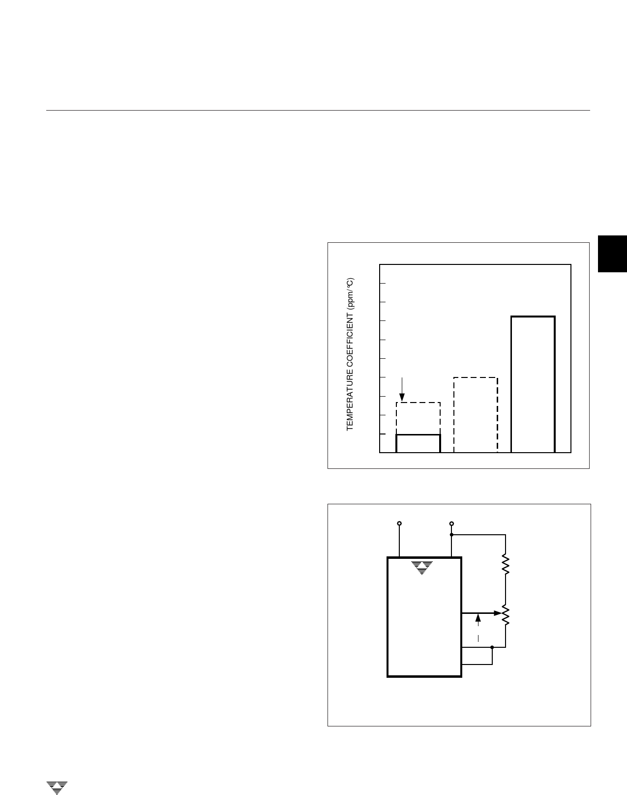
Internal Voltage Reference Stability
2 The analog common voltage temperature stability has
been significantly improved (Figure 10). The “A” version of
the industry standard circuits allow users to upgrade old
systems and design new systems without external voltage
references. External R and C values do not need to be
changed. Figure 11 shows analog common supplying the
necessary voltage reference for the TC7106A/TC7107A.
3
200
180
NO
MAXIMUM
160
SPECIFIED
140
120
NO MAXIMUM
SPECIFIED
TYPICAL
100
NO MAXIMUM
MAXIMUM SPECIFIED
80
LIMIT
TYPICAL
60
TYPICAL
40
20
TC
7106A
ICL7106
ICL7136
0
4
5
Figure 10. Analog Common Temperature Coefficient
1
V–
V+
TC7106A
TC7107A
VR+EF 36
VR– EF
ANALOG
COMMON
VREF
35
32
24kΩ
1kΩ
SET VREF = 1/2 VFULL SCALE
Figure 11. Internal Voltage Reference Connection
6
7
8
TELCOM SEMICONDUCTOR, INC.
3-195
Share Link: 