TC7129(2002) データシートの表示(PDF) - Microchip Technology
部品番号
コンポーネント説明
メーカー
TC7129
(Rev.:2002)
(Rev.:2002)
Microchip Technology

TC7129 Datasheet PDF : 24 Pages
| |||
TC7129
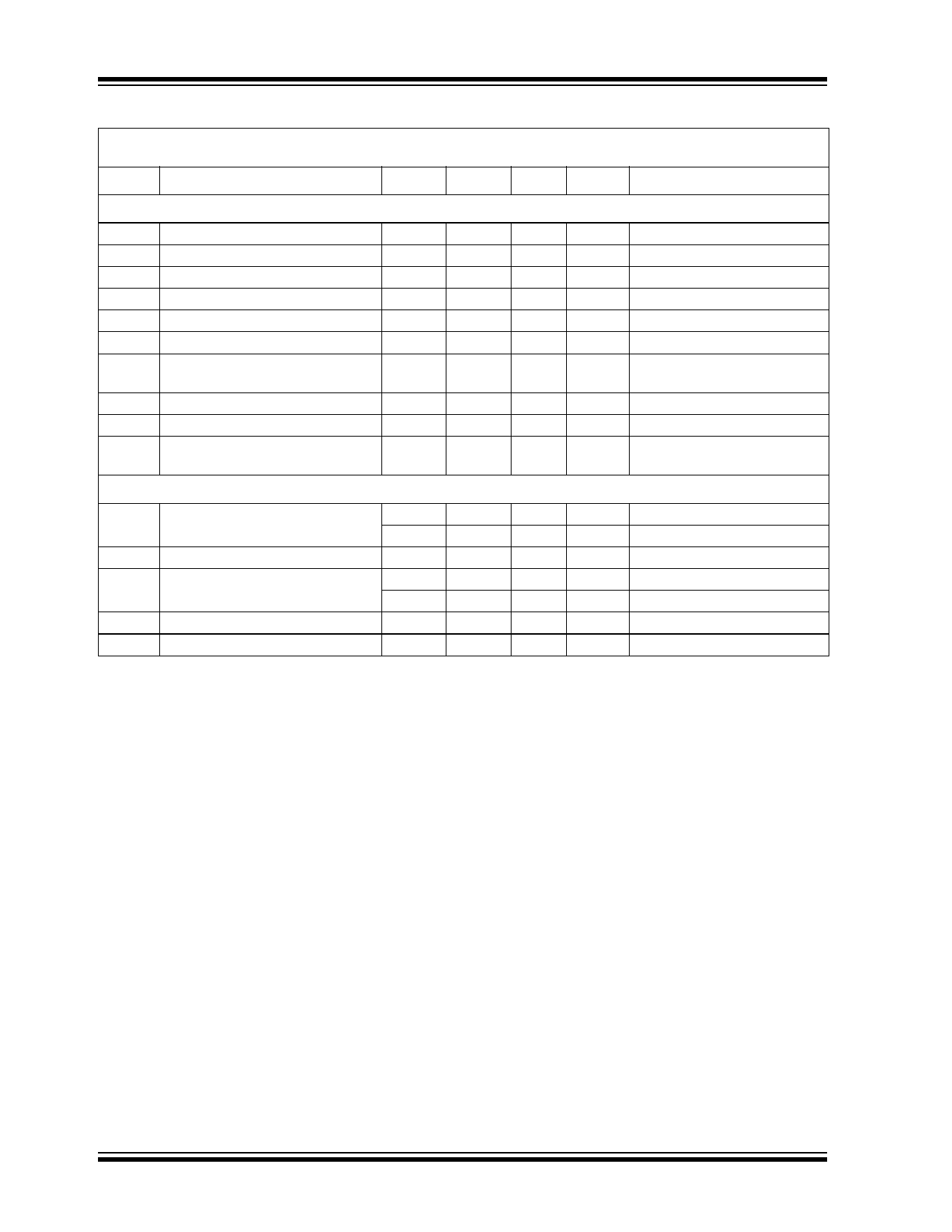
TC7129 ELECTRICAL SPECIFICATIONS (CONTINUED)
Electrical Characteristics: V+ to V- = 9V, VREF = 1V, TA = +25°C, fCLK = 120kHz, unless otherwise indicated.
Pin numbers refer to 40-pin DIP.
Symbol
Parameter
Min
Typ
Max
Unit
Test Conditions
fCLK
Clock Frequency
—
VDISP Resistance
—
Low Battery Flag Activation Voltage
6.3
120
360
kHz
50
—
kΩ
VDISP to V+
7.2
7.7
V
V+ to V-
Digital
Continuity Comparator Threshold
Voltages
Pull-down Current
100
200
—
mV VOUT Pin 27 = High
—
200
400
mV VOUT Pin 27 = Low
—
2
10
µA Pins 37, 38, 39
"Weak Output" Current
Sink/Source
—
3/3
—
µA Pins 20, 21 Sink/Source
—
3/9
—
µA Pin 27 Sink/Source
Pin 22 Source Current
—
40
—
µA
Pin 22 Sink Current
—
3
—
µA
Note 1: Input voltages may exceed supply voltages, provided input current is limited to ±400µA. Currents above this value may
result in invalid display readings, but will not destroy the device if limited to ±1mA. Dissipation ratings assume device is
mounted with all leads soldered to printed circuit board.
DS21459B-page 4
© 2002 Microchip Technology Inc.
Share Link: