TDA8769HW データシートの表示(PDF) - Philips Electronics
部品番号
コンポーネント説明
メーカー
TDA8769HW
Philips Electronics

TDA8769HW Datasheet PDF : 28 Pages
| |||
Philips Semiconductors
12-bit, 60/80/105 Msps Analog-to-Digital Converter
(ADC) Nyquist/high IF sampling
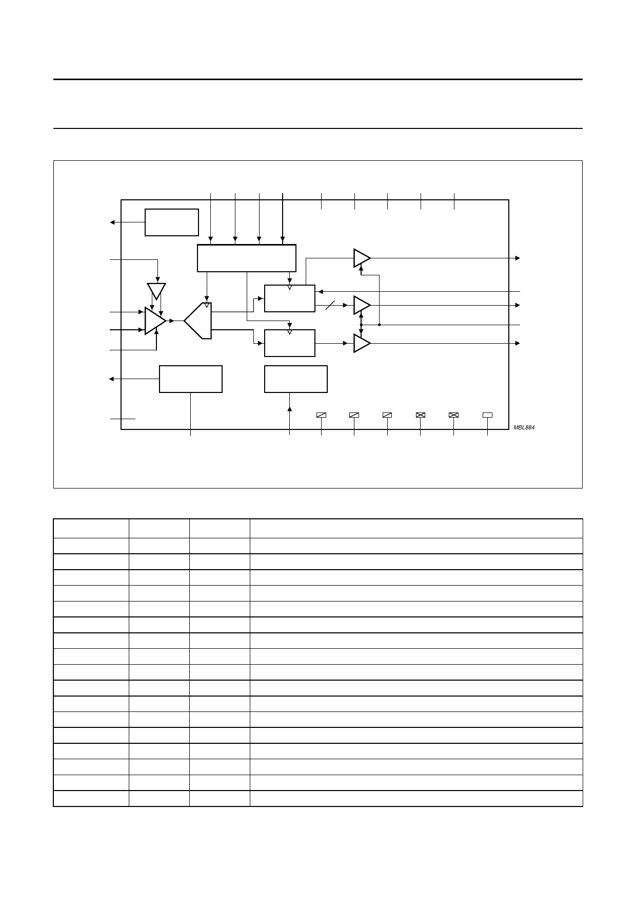
6 BLOCK DIAGRAM
Objective specification
TDA8769
handbook, full pagewidth
FSREF 13
VREF 11
DEL0 DEL1 CLK CLKN
16 15 39 38
VREF
REFERENCE
CLOCK
DRIVER
VCCA1 VCCA3 VCCA4 VCCD1 VCCD2
2
3
44
40
17
TDA8769
36 CCS
AMP TRACK
INN 47
IN
46
&
ADC
TH 42
HOLD
LATCH
12
LATCH
19
23 to 34
35
22
OTC
D0 to D11
VCCO
IR
CMADC
n.c.
1
CMADC
REFERENCE
6 to 10, 12,
14, 21, 45
5
DEC
POWER
MANAGEMENT
20
48
4
43
41
18
37
CEN AGND1 AGND3 AGND4 DGND1 DGND2 OGND
MBL884
Fig.1 Block diagram.
7 PINNING
SYMBOL
CMADC
VCCA1
VCCA3
AGND3
DEC
n.c.
n.c.
n.c.
n.c.
n.c.
VREF
n.c.
FSREF
n.c.
DEL1
DEL0
VCCD2
2003 Dec 09
PIN
TYPE(1)
DESCRIPTION
1
O
regulator output common mode ADC output
2
P
analog supply voltage 1 (5.0 V)
3
P
analog supply voltage 3 (5.0 V)
4
G
analog ground 3
5
I/O
decoupling node
6
−
not connected
7
−
not connected
8
−
not connected
9
−
not connected
10
−
not connected
11
I
reference voltage input
12
−
not connected
13
O
reference output
14
−
not connected
15
I
complete conversion sampling delay input 1
16
I
complete conversion sampling delay input 0
17
P
digital supply voltage 2 (5.0 V)
4
Share Link: