TS39100CP50ROG データシートの表示(PDF) - TSC Corporation
部品番号
コンポーネント説明
メーカー
TS39100CP50ROG Datasheet PDF : 7 Pages
| |||
TS39100
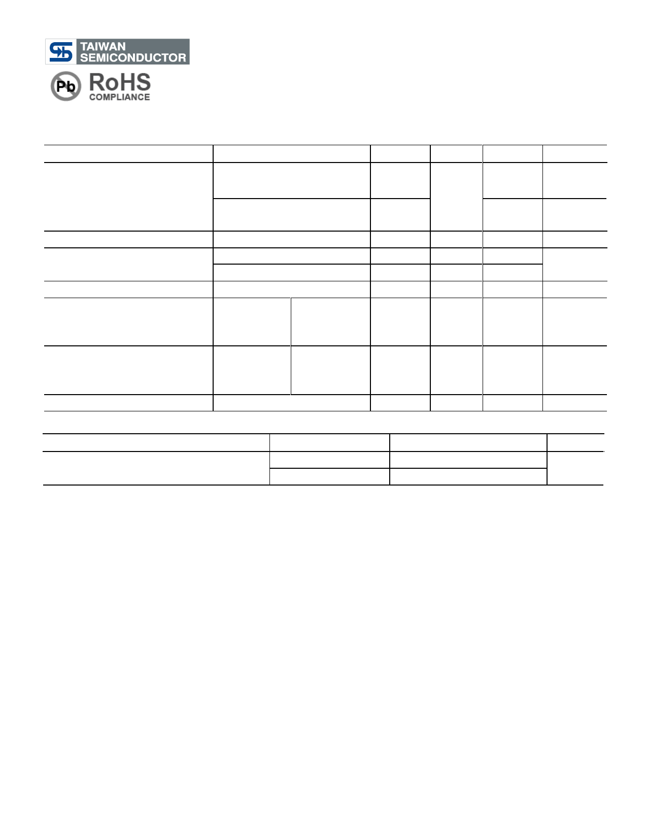
1A Ultra Low Dropout Voltage Regulator
Electrical Characteristics
VIN = VOUT + 1V, VIN =2.5V for fixed reference output voltage, Venable= 2.25V, Ta = 25oC, unless otherwise specified.
Parameter
Conditions
Min
Typ
Max
Unit
Output Voltage
Line Regulation
Load Regulation
Output Voltage Temp. Coefficient
Dropout Voltage (Note 5)
Quiescent Current (Note 6)
Current Limited
10mA ≤ IL ≤ 1.0A,
Vo+1V ≤ VIN ≤ 8V
10mA ≤ IL ≤ 1.0A,
2.5V ≤ VIN ≤ 16V
IL=10mA, Vo+1V ≤ VIN ≤ 16V
VIN =Vout+1V, 8mA≤IL≤300mA
VIN =Vout+1V, 10mA≤IL≤1A
IL=100mA
ΔVOUT = -1% IL=500mA
IL=1.0A
IL=100mA
VIN= VOUT +1V IL=500mA
IL=1.0A
VOUT =0, VIN = VOUT +1V
0.980|Vo|
0.970|Vo|
--
--
--
--
--
--
--
--
--
--
--
VOUT
0.05
0.05
0.2
40
100
275
400
0.7
4.0
12.0
1.8
1.020|Vo|
V
1.030|Vo|
0.5
0.1
1.0
100
250
350
630
2
6
20
--
V
%
%
ppm/ oC
mV
mA
A
Thermal Performance
Condition
Package type
Typ
Unit
Thermal Resistance Junction to Case
SOT-223
TO-252
15
oC/W
10
Note 1: Absolute Maximum Rating is limits beyond which damage to the device may occur. For guaranteed
specifications and test conditions see the Electrical Characteristics.
Note 2: The device is not guaranteed to operate outside its operating rating.
Note 3: Devices are ESD sensitive. Handling precautions recommended.
Note 4: The maximum allowable power dissipation is a function of the maximum junction temperature, TJ, the junction
to ambient thermal resistance, ӨJA, and the ambient temperature, Ta. Exceeding the maximum allowable
power dissipation will cause excessive die temperature, and the regulator will go into thermal shutdown. The
effective value of ӨJA can be reduced by using a heat sink, Pd(max) = (TJ(max) – Ta) / ӨJA.
Note 5: Dropout voltage is defined as the input to output differential at which the output voltage drops -1% below its
nominal value measured at 1V differential.
Note 6: Ground pin current is the regulator quiescent current. The total current drawn from the source is the sum of the
ground pin current and output load current, IGND = IIN - IOUT for fix output voltage, , IGND = IIN - IOUT +10mA for fix
reference output voltage in full load regulation.
Note 8: Output voltage temperature coefficient is ΔVOUT (worse cast) / (TJ(max) – TJ(MIN)) where is TJ(max) +125oC and
TJ(MIN) is 0oC.
2/7
Version: B08
Share Link: 