TSA5060AT データシートの表示(PDF) - Philips Electronics
部品番号
コンポーネント説明
メーカー
TSA5060AT Datasheet PDF : 24 Pages
| |||
Philips Semiconductors
1.3 GHz I2C-bus controlled low phase
noise frequency synthesizer
Product specification
TSA5060A
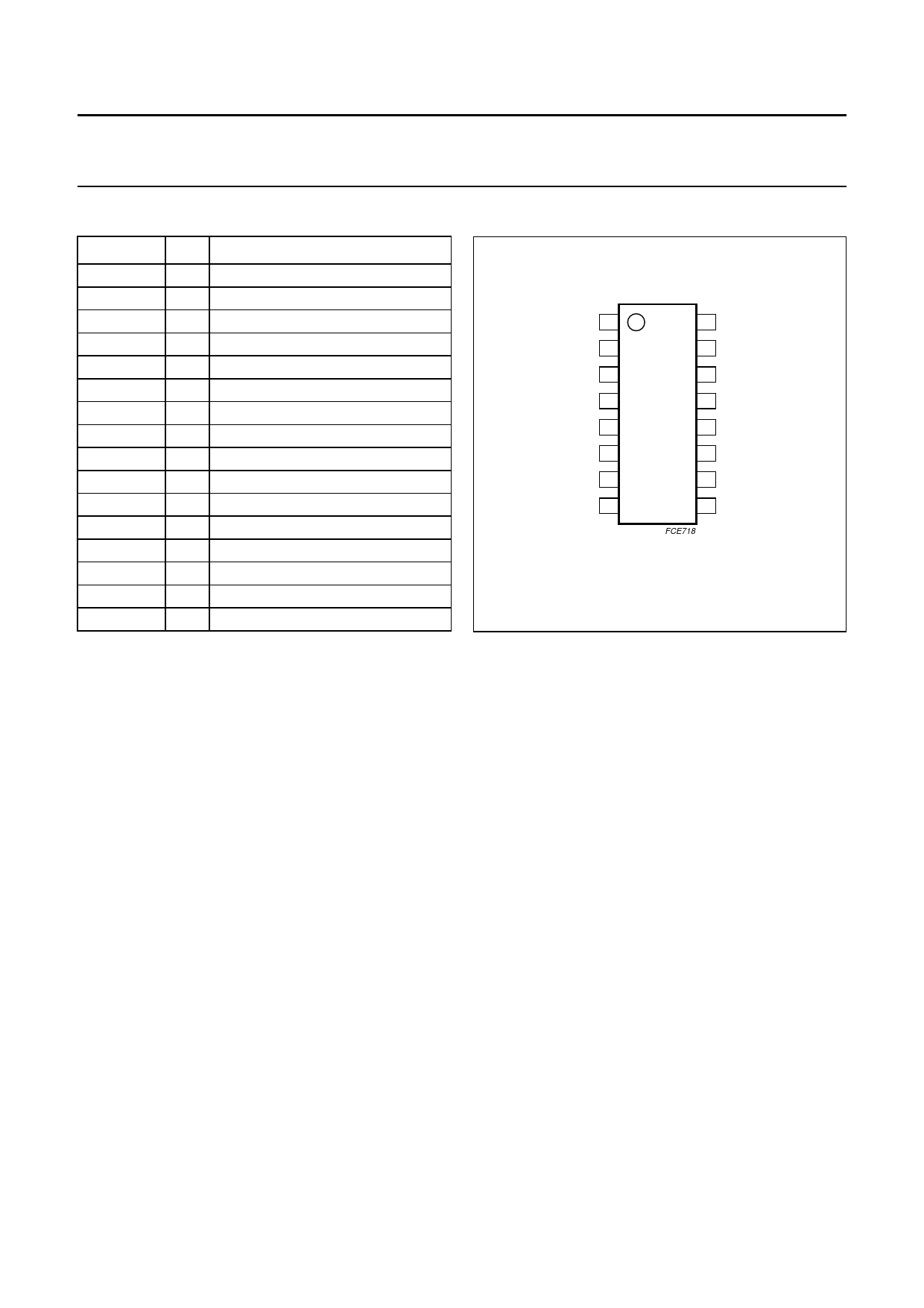
PINNING
SYMBOL
CP
XTAL
XT/COMP
AS
SDA
SCL
P3
P2
P1
P0
ADC
VCC
RFA
RFB
GND
DRIVE
PIN
DESCRIPTION
1 charge pump output
2 crystal oscillator input
3 fxtal or fcomp signal output
4 I2C-bus address selection input
5 I2C-bus serial data input/output
6 I2C-bus serial clock input
7 general purpose output Port 3
8 general purpose input/output Port 2
9 general purpose input/output Port 1
10 general purpose input/output Port 0
11 analog-to-digital converter input
12 supply voltage
13 RF signal input A
14 RF signal input B
15 ground
16 external NPN drive output
handbook, halfpage
CP 1
16 DRIVE
XTAL 2
15 GND
XT/COMP 3
14 RFB
AS 4
13 RFA
TSA5060A
SDA 5
12 VCC
SCL 6
11 ADC
P3 7
10 P0
P2 8
9 P1
FCE718
Fig.2 Pin configuration.
FUNCTIONAL DESCRIPTION
The TSA5060A contains all the necessary elements
except a reference source, a loop filter and an external
NPN transistor to control a varicap tuned local oscillator
forming a phase locked loop frequency synthesized
source. The IC is designed in a high speed process with a
fast phase detector to allow a high comparison frequency
to reach a low phase noise level on the oscillator.
The block diagram is shown in Fig.1. The RF signal is
applied at pins RFA and RFB. The input preamplifier
provides a good sensitivity. The output of the preamplifier
is fed to the 17-bit programmable divider either through a
divide-by-two prescaler or directly. Because of the internal
high speed process, the RF divider is working at a
frequency up to 1.3 GHz, without the need for the
divide-by-two prescaler to be used.
The output of the 17-bit programmable divider fDIV is fed
into the phase comparator, where it is compared in both
phase and frequency with the comparison frequency fcomp.
This frequency is derived from the signal present at
pin XTAL, fxtal, divided down in the reference divider. It is
possible either to connect a quartz crystal to pin XTAL and
then using the on-chip crystal oscillator, or to feed this pin
with a reference signal from an external source.
The reference divider can have a dividing ratio selected
from 16 different values between 2 and 320, including the
ratio 24 to cope with the offset requirement of the UK-DTT
system, see Table 8.
The output of the phase comparator drives the
charge pump and the loop amplifier section. This amplifier
requires the use of an external NPN transistor. Pin CP is
the output of the charge pump, and pin DRIVE is
connected to the base of the external transistor. This
transistor has its emitter grounded and the collector drives
the tuning voltage to the varicap diode of the Voltage
Controlled Oscillator (VCO). The loop filter has to be
connected between pin CP and the collector of the
external NPN transistor (see Fig.4).
It is also possible to drive another PLL synthesizer, or the
clock input of a digital demodulation IC, from
pin XT/COMP. It is possible to select by software either
fxtal, the crystal oscillator frequency or fcomp, the frequency
present after the reference divider. It is also possible to
switch off this output, in case it is not used.
For test and alignment purposes, it is possible to release
the drive output to be able to apply an external voltage on
it, to select one of the three charge pump test modes, and
to monitor half the fDIV at Port P0. See Table 10 for all
possible modes.
Four open-collector output ports are provided on the IC for
general purpose; three of these can also be used as input
ports. A 3-bit ADC is also available.
2000 Oct 24
5
Share Link: 