UPD3777CY „Éá„Éľ„āŅ„ā∑„Éľ„Éą„ĀģŤ°®Á§ļÔľąPDFÔľČ - NEC => Renesas Technology
ťÉ®ŚďĀÁē™ŚŹ∑
„ā≥„É≥„ÉĚ„Éľ„Éć„É≥„ÉąŤ™¨śėé
„É°„Éľ„āę„Éľ
UPD3777CY Datasheet PDF : 20 Pages
| |||
¬Ķ PD3777
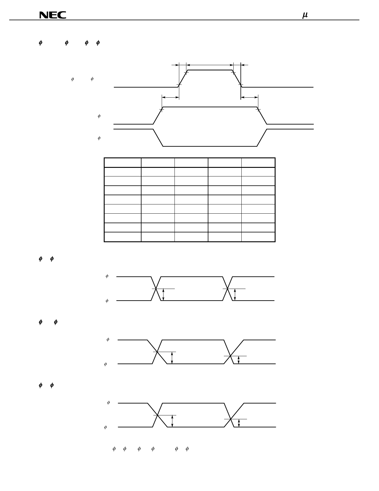
ŌÜ TG1 to ŌÜ TG3, ŌÜ 1, ŌÜ 2 TIMING CHART
ŌÜ TG1 to ŌÜ TG3
t8
t7
t9
90 %
10 %
t10
t11
90 %
ŌÜ1
ŌÜ2
Symbol
t1, t2
t1’, t2’
t3
t4
t5, t6
t7
t8, t9
t10, t11
ŌÜ 1, ŌÜ 2 cross points
ŌÜ1
ŌÜ2
ŌÜ 1L, ŌÜ 2 cross points
ŌÜ2
ŌÜ 1L
ŌÜ 1, ŌÜ 2L cross points
ŌÜ1
ŌÜ 2L
MIN.
TYP.
MAX.
Unit
0
50
‚ąí
ns
0
5
‚ąí
ns
20
150
‚ąí
ns
130
300
‚ąí
ns
0
50
‚ąí
ns
3000
10000
‚ąí
ns
0
50
‚ąí
ns
900
1000
‚ąí
ns
2 V or more
2 V or more
2 V or more
0.5 V or more
2 V or more
0.5 V or more
Remark Adjust cross points (ŌÜ 1, ŌÜ 2), (ŌÜ 1L, ŌÜ 2) and (ŌÜ 1, ŌÜ 2L) with input resistance of each pin.
Data Sheet S14583EJ1V0DS00
9
Share Link: 