UPSD3253B-40 データシートの表示(PDF) - STMicroelectronics
部品番号
コンポーネント説明
メーカー
UPSD3253B-40
STMicroelectronics

UPSD3253B-40 Datasheet PDF : 176 Pages
| |||
µPSD325X DEVICES
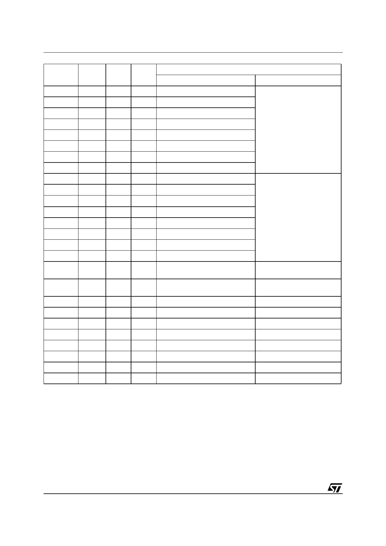
Port Pin
PB0
PB1
PB2
PB3
PB4
PB5
PB6
PB7
PC0
PC1
PC2
PC3
PC4
PC5
PC6
PC7
PD1
Signal
Name
TMS
TCK
VSTBY
TSTAT
TERR
TDI
TDO
Pin No.
80
78
76
74
73
72
67
66
20
16
15
14
9
7
6
5
In/Out
I/O
I/O
I/O
I/O
I/O
I/O
I/O
I/O
I
I
I/O
I/O
I/O
I
O
I/O
Basic
General I/O port pin
General I/O port pin
General I/O port pin
General I/O port pin
General I/O port pin
General I/O port pin
General I/O port pin
General I/O port pin
JTAG pin
JTAG pin
General I/O port pin
General I/O port pin
General I/O port pin
JTAG pin
JTAG pin
General I/O port pin
CLKIN
3
I/O General I/O port pin
PD2
Vcc
Vcc
GND
GND
GND
NC
NC
NC
CSI
1
I/O General I/O port pin
12
50
13
29
69
11
17
71
Function
Alternate
1. PLD Macro-cell outputs
2. PLD inputs
3. Latched Address Out (A0-A7)
1. PLD Macro-cell outputs
2. PLD inputs
3. SRAM stand by voltage input
(VSTBY)
4. SRAM battery-on indicator
(PC4)
5. JTAG pins are dedicated pins
1. PLD I/O
2. Clock input to PLD and APD
1. PLD I/O
2. Chip select to PSD Module
52 PIN PACKAGE I/O PORT
The 52-pin package members of the µPSD325X
devices have the same port pins as those of the
80-pin package except:
s Port 0 (P0.0-P0.7, external address/data bus
AD0-AD7)
s Port 2 (P2.0-P2.3, external address bus A8-
A11)
s Port A (PA0-PA7)
s Port D (PD2)
s Bus control signal (RD,WR,PSEN,ALE)
Pin 5 requires a pull-up resistor (2kΩ for 3V de-
vices, 7.5kΩ for 5V devices) for all devices, with
or without USB function.
16/176
Share Link: