VRE3050 データシートの表示(PDF) - Unspecified
部品番号
コンポーネント説明
メーカー
VRE3050 Datasheet PDF : 8 Pages
| |||
ABSOLUTE MAXIMUM RATINGS
Power Supply ………………………-0.3V to +40V
OUT, TRIM …………………………-0.3V to +12V
NR……………………………………-0.3V to +6V
Operating Temp. (A,B,C)……………0°C to 70°C
Operating Temp. (J,K,L)……………-40°C to 85°C
Out Short Circuit to GND Duration (VIN< 12V)…...Continuous
Out Short Circuit to GND Duration (VIN< 40V)…….……5 sec
Out Short Circuit to IN Duration (VIN< 12V)………Continuous
Continuous Power Dissipation (TA = +70°C)………...300mW
Storage Temperature……………………..……-65°C to 150°C
Lead Temperature (soldering,10 sec)…………………..250°C
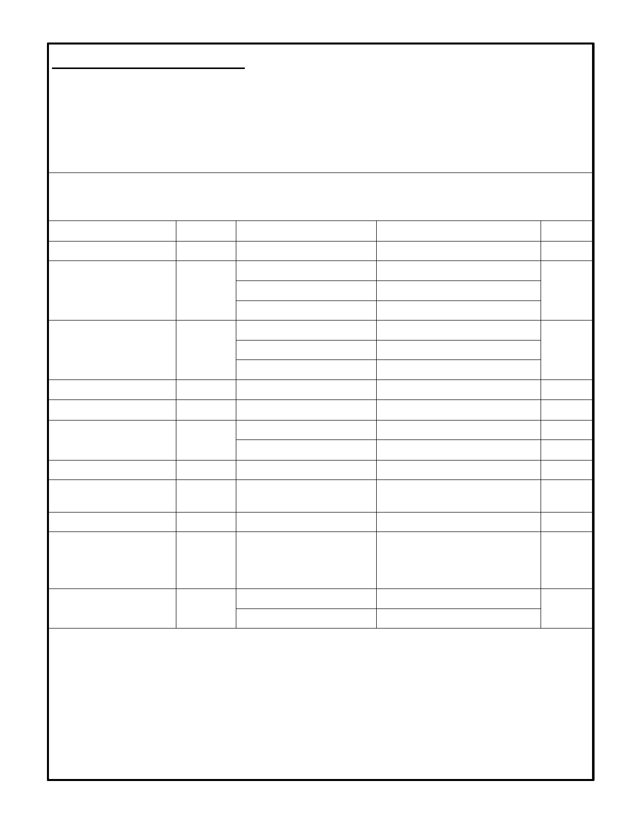
ELECTRICAL SPECIFICATIONS
Vps =+10V, T = 25°C, Iout=0mA unless otherwise noted.
PARAMETER
Input Voltage
SYMBOL
VIN
Output Voltage
VOUT
(Note 1)
Output Voltage
Temperature Coefficient
(Note 2)
Trim Adjustment Range
Turn-On Settling Time
Output Noise Voltage
Temperature Hysterisis
TCVOUT
∆VOUT
Ton
en
CONDITIONS
VRE3050A/J
VRE3050B/K
VRE3050C/L
VRE3050A/J
VRE3050B/K
VRE3050C/K
Figure 3
To 0.01% of final value
0.1Hz<f<10Hz
10Hz<f<1kHz
Note 4
Long Term Stability
∆VOUT/t
Supply Current
Load Regulation
(Note 3)
Line Regulation
(Note 3)
IIN
∆VOUT/
∆IOUT
∆VOUT/
∆VIN
Sourcing:
0mA ≤ IOUT ≤ 15mA
Sinking:
-15mA ≤ IOUT ≤0mA
8V ≤ VIN ≤ 10V
10V ≤ VIN ≤18V
Notes:
1) The specified values are without external trim.
2) The temperature coefficient is determined by the
box method. See discussion on temperature
performance.
3) Line and load regulation are measured with pulses and
do not include voltage changes due to temperature.
4) Hysterisis over the operating temperature range.
MIN TYP MAX
8
36
4.9995 5.0000 5.0005
4.9992 5.0000 5.0008
4.9990 5.0000 5.0010
0.3
0.6
0.5
1.0
1.0
2.0
±5
2
3.0
2.5
5.0
1
6
3.5
4.0
8
12
8
12
25
35
5
10
UNITS
V
V
ppm/°C
mV
µs
µVp-p
µVRMS
ppm
ppm/
1khrs
mA
ppm/
mA
ppm/V
VRE3050DS REV. D JULY 2000
Share Link: 