XE1202I027 データシートの表示(PDF) - Unspecified
部品番号
コンポーネント説明
メーカー
XE1202I027 Datasheet PDF : 26 Pages
| |||
Data Sheet
XE1202
5 Interface definition, Principles of operation
5.1 Serial Control Interface
A 3-wire bi-directional bus (SCK, SI, SO) is used to program the XE1202 and read data from it. SCK and SI are
input signals, for example generated by a microcontroller. SO is an output signal controlled by the XE1202. In write
mode, at the falling edge of the SCK signal, the logic data on the SI line is written into an internal shift register. In
read mode, at the rising edge of the SCK signal, the data on the SO line become valid and should be sampled at
the next falling edge of SCK.
The signal EN must be low during the whole write and read sequences. In write mode the actual content of the
configuration register is updated at the rising edge of the EN signal. Before this, the new data is stored in temporary
registers whose content does not affect the transceiver settings.
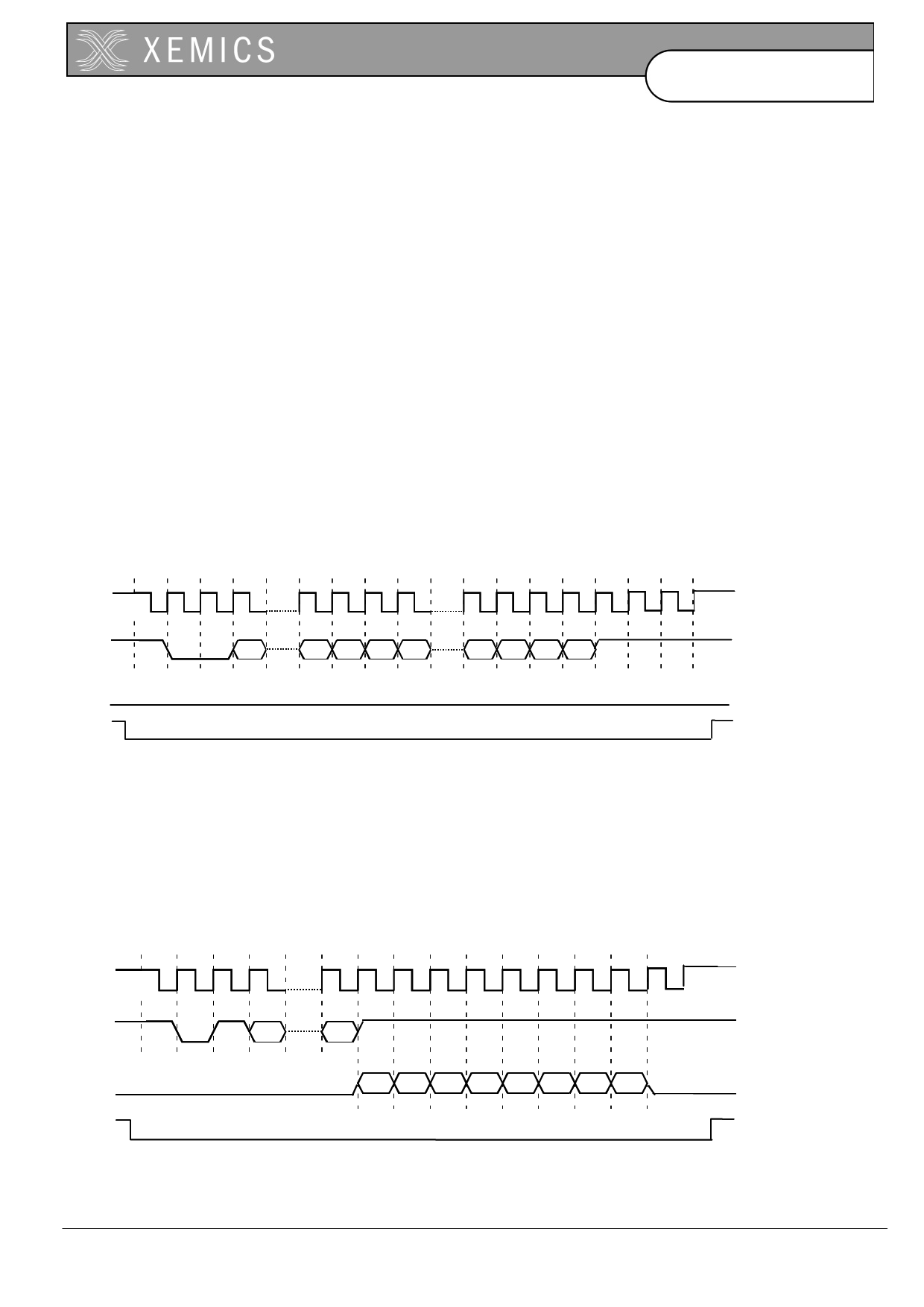
The time diagram of a write sequence is given in the figure below. The sequence is initiated when a Start condition
is detected, that is when the SI signal is set to “0” during a period of SCK. The next bit is a read/write (R/W) bit
which should be “0” to indicate a write operation. The next 5 bits are the address of the control register A[4:0] to be
accessed, MSB first. Then, the next 8 bits are the data to be written in the register. The sequence ends with 2 stop
bits set to “1”. The data on SI should change at the rising edges of SCK, and are sampled at the falling edge of
SCK. After the 2 stop bits, the data transfer is terminated, even if the SI line stays at “1”. After this the SI line should
be at “1” for at least one clock cycle on SCK before a new write or read sequence can start. In doing this, users can
write multiple registers in raw, there is no need to raise the EN signal in between. The duty cycle of SCK must be
between 40 % and 60 % and the maximum frequency of this signal is 1 MHz. Over the operating supply and
temperature range, set-up and hold time for SI on the falling edge of SCK are 200ns.
SCK
SI
START R/W A(4)
A(1) A(0) D(7) D(6)
D(3) D(2) D(1) D(0) STOP STOP
SO
EN
Figure 5 Write sequence into configuration register
The time diagram of a read sequence is given in figure below. The sequence is initiated when a Start condition is
detected, that is when the SI signal is set to “0” during a period of SCK. The next bit is a read/write (R/W) bit which
should be “1” to indicate a read operation. The next 5 bits are the address of the control register A[4:0] to be
accessed, MSB first. Then the data from the register are transmitted on the SO pin. The data become valid at the
rising edges of SCK and should be sampled at the falling edge of SCK. After this the data transfer is terminated.
The SI line must stay high for at least one clock cycle on SCK to start a new write or read sequence. The maximum
current drive on SO is 2mA @ 2.7V, the maximum load is CLop.
SCK
SI
SO
EN
START R/W A(4)
A(0)
D(7) D(6) D(5) D(4) D(3) D(2) D(1) D(0)
Figure 6 Read sequence into configuration register
13
D0211-105
Share Link: 