XE1203 データシートの表示(PDF) - Unspecified
部品番号
コンポーネント説明
メーカー
XE1203 Datasheet PDF : 37 Pages
| |||
Data Sheet
XE1203
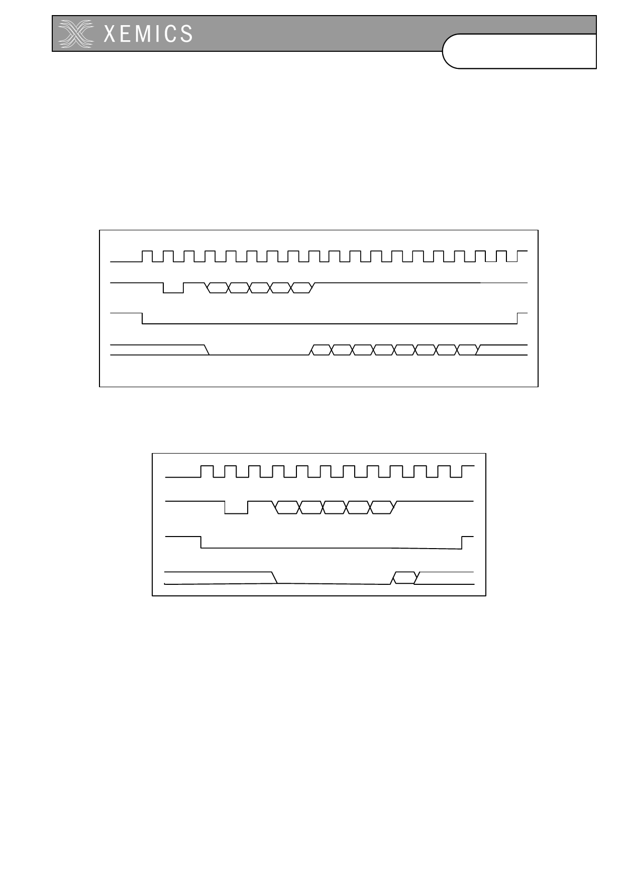
The time diagram of a read sequence is given in figure below. The sequence is initiated when a Start condition is
detected, that is when the SI signal is set to “0” during a period of SCK. The next bit is a read/write (R/W) bit which
should be “1” to indicate a read operation. The next 5 bits are the address of the control register A[4:0] to be
accessed, MSB first. Then the data from the register are transmitted on the SO pin. The data become valid at the
rising edges of SCK and should be sampled at the falling edge of SCK. After this, the data transfer is terminated.
The SI line must stay high for at least one clock cycle on SCK to start a new write or read sequence. The maximum
current drive on SO is 2mA @ 2.7V, the maximum load is CLop.
When the serial interface is not used for read or write operations, both SCK and SI should be set to “1”. Except in
read mode, SO is set to “HZ”.
SCK
SI
EN
SO
HZ
A4 A3 A2 A1 A0
D7 D6 D5 D4 D3 D2 D1 D0
HZ
Figure 13 Read sequence of configuration register.
When reading the register at address zero, the timing diagram is the following one.
SCK
SI
A4 A3 A2 A1 A0
EN
SO
HZ
D7 HZ
Figure 14 Read sequence of configuration register at address 0.
5.2 CONFIGURATION AND STATUS REGISTERS
The transceiver has several operating modes and parameters, which can be selected by the user. Some of these
modes and all the parameters are stored in an internal configuration register that can be accessed by the
microcontroller through a 3-wires serial interface. The switching option allows some parameters to be changed
rapidly; defined in SWParam registers, by using the 3-wire interface in a reduced sequence or by using a single
input pin SWITCH.
The configuration is defined by the Chip_Config parameter (address 0) when RTParam_Switch_ext is low or by the
pad SWITCH when RTParam_Switch_ext is high. Using Chip_config or SWITCH allows switching between a set of
two predefined parameters of the transceiver. If a parameter must not change then it must be set at the same value
in the two registers used to define it. To switch between configurations, the new value of Chip_config or SWITCH
should be modified when the EN signal is low. The actual change will be applied to the transceiver upon the rising
edge of the EN signal. The following table summarizes the chip configuration programming.
20
D0308-214
Share Link: 