ATT3042 データシートの表示(PDF) - Unspecified
部品番号
コンポーネント説明
メーカー
ATT3042 Datasheet PDF : 80 Pages
| |||
ATT3000 Series Field-Programmable Gate Arrays
Data Sheet
February 1997
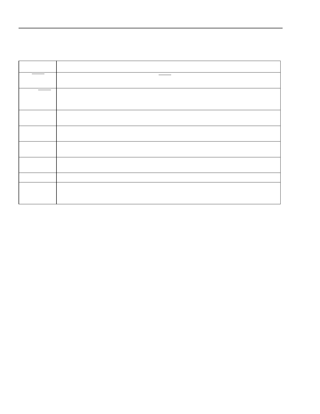
Pin Information (continued)
Table 5. I/O Pins with Special Functions (continued)
Symbol
RCLK
RDY/BUSY
D[7:0]
A[15:0]
DIN
DOUT
TCLKIN
I/O
Name/Description
During master parallel mode configuration, RCLK represents a read of an external dynamic
memory device (normally not used).
During peripheral parallel mode configuration, this pin indicates when the chip is ready for
another byte of data to be written to it. After configuration is complete, this pin becomes a user-
programmed I/O pin.
This set of eight pins represents the parallel configuration byte for the parallel master and
peripheral modes. After configuration is complete, they are user-programmed I/O pins.
This set of 16 pins presents an address output for a configuration EPROM during master parallel
mode. After configuration is complete, they are user-programmed I/O pins.
This user I/O pin is used as serial data input during slave or master serial configuration. This pin
is data zero input in master or peripheral configuration mode.
This user I/O pin is used during configuration to output serial configuration data for daisy-
chained slaves’ data in.
This is a direct CMOS level input to the global clock buffer.
Input/Output (Unrestricted). May be programmed by the user to be input and/or output pin
following configuration. Some of these pins present a high-impedance pull-up (see next page) or
perform other functions before configuration is complete (see above).
36
Lucent Technologies Inc.
Share Link: 