AM27C256-255DIB データシートの表示(PDF) - Advanced Micro Devices
部品番号
コンポーネント説明
メーカー
AM27C256-255DIB Datasheet PDF : 12 Pages
| |||
FINAL
Am27C256
256 Kilobit (32,768 x 8-Bit) CMOS EPROM
Advanced
Micro
Devices
DISTINCTIVE CHARACTERISTICS
s Fast access time
— 55 ns
s Low power consumption
— 20 µA typical CMOS standby current
s JEDEC-approved pinout
s Single +5 V power supply
s ±10% power supply tolerance available
s 100% Flashrite programming
— Typical programming time of 4 seconds
GENERAL DESCRIPTION
The Am27C256 is a 256K-bit ultraviolet erasable pro-
grammable read-only memory. It is organized as 32K
words by 8 bits per word, operates from a single +5 V
supply, has a static standby mode, and features fast sin-
gle address location programming. Products are avail-
able in windowed ceramic DIP packages as well as plas-
tic one time programmable (OTP) PDIP, TSOP, and
PLCC packages.
Typically, any byte can be accessed in less than 55 ns,
allowing operation with high-performance microproces-
sors without any WAIT states. The Am27C256 offers
separate Output Enable (OE) and Chip Enable (CE)
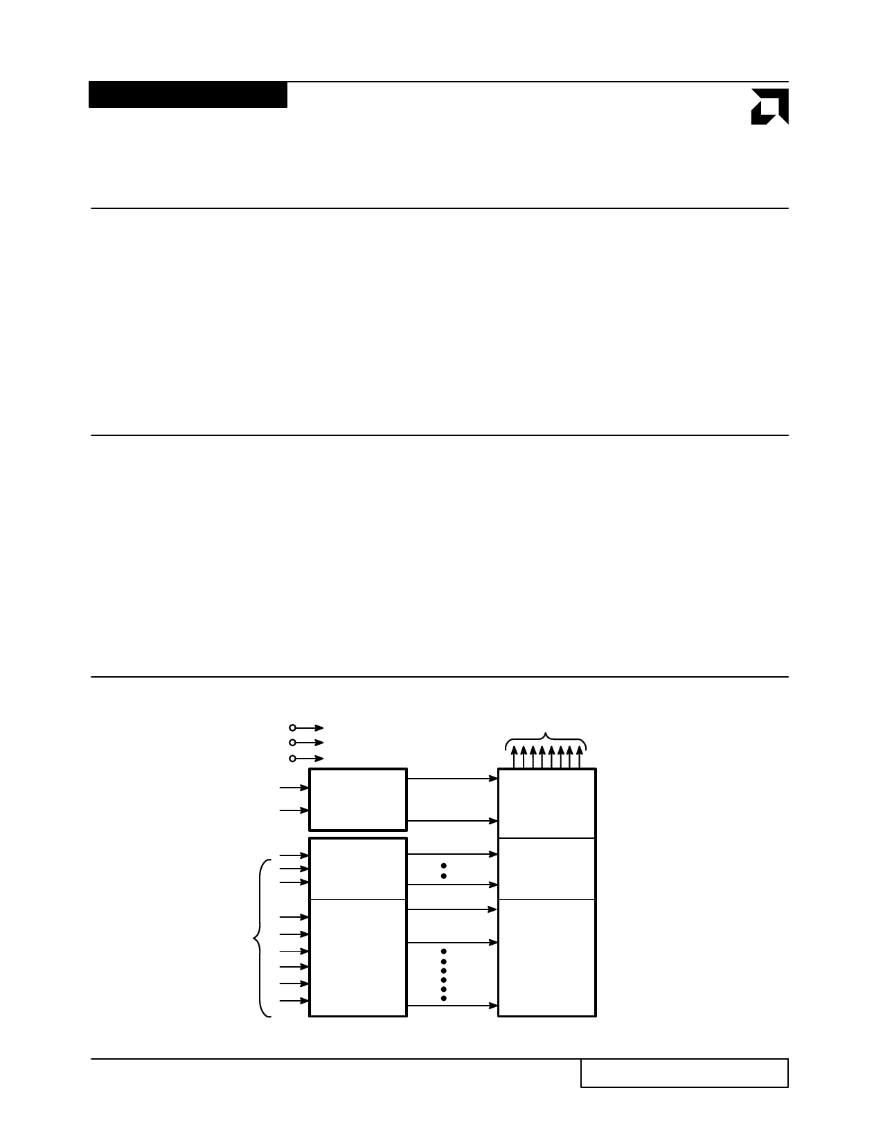
BLOCK DIAGRAM
VCC
VSS
VPP
OE
Output Enable
Chip Enable
CE
and
Prog Logic
s Latch-up protected to 100 mA from –1 V to
VCC + 1 V
s High noise immunity
s Versatile features for simple interfacing
— Both CMOS and TTL input/output
compatibility
— Two line control functions
s Standard 28-pin DIP, PDIP, 32-pin TSOP and
PLCC packages
controls, thus eliminating bus contention in a multiple
bus microprocessor system.
AMD’s CMOS process technology provides high speed,
low power, and high noise immunity. Typical power con-
sumption is only 80 mW in active mode, and 100 µW in
standby mode.
All signals are TTL levels, including programming sig-
nals. Bit locations may be programmed singly, in blocks,
or at random. The Am27C256 supports AMD’s Flashrite
programming algorithm (100 µs pulses) resulting in typi-
cal programming time of 4 seconds.
Data Outputs
DQ0–DQ7
Output
Buffers
Y
Decoder
Y
Gating
A0–A14
Address
Inputs
X
Decoder
262,144
Bit Cell
Matrix
2-32
08007H-1
Publication# 08007 Rev. H Amendment /0
Issue Date: May 1995
Share Link: 