HM628512C „Éá„Éľ„āŅ„ā∑„Éľ„Éą„ĀģŤ°®Á§ļÔľąPDFÔľČ - Renesas Electronics
ťÉ®ŚďĀÁē™ŚŹ∑
„ā≥„É≥„ÉĚ„Éľ„Éć„É≥„ÉąŤ™¨śėé
„É°„Éľ„āę„Éľ
HM628512C Datasheet PDF : 19 Pages
| |||
HM628512C Series
Low VCC Data Retention Characteristics (Ta = ‚Äď20 to +70¬įC)
Parameter
Symbol Min Typ Max Unit Test conditions*3
VCC for data retention
Data retention current
VDR
I CCDR
2
‚ÄĒ‚ÄĒ
V
‚ÄĒ 0.8*4 20*1 ¬ĶA
‚ÄĒ 0.8*4 10*2 ¬ĶA
CS ‚Č• VCC ‚Äď 0.2 V, Vin ‚Č• 0 V
VCC = 3.0 V, Vin ‚Č• 0 V
CS ‚Č• VCC ‚Äď 0.2 V
Chip deselect to data retention time tCDR
0
‚ÄĒ‚ÄĒ
ns
See retention waveform
Operation recovery time
tR
tRC*5 ‚ÄĒ
‚ÄĒ
ns
Notes: 1. For L-version and 10 ¬ĶA (max.) at Ta = ‚Äď20 to +40¬įC.
2. For L-SL-version and 3 ¬ĶA (max.) at Ta = ‚Äď20 to +40¬įC.
3. CS controls address buffer, WE buffer, OE buffer, and Din buffer. In data retention mode, Vin
levels (address, WE, OE, I/O) can be in the high impedance state.
4. Typical values are at VCC = 3.0 V, Ta = +25¬įC and specified loading, and not guaranteed.
5. tRC = read cycle time.
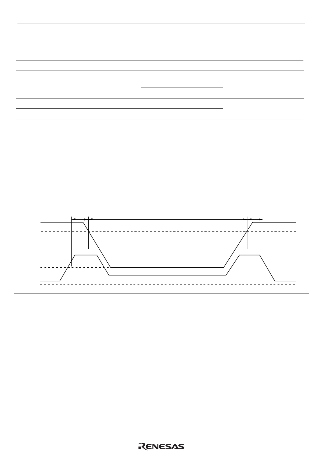
Low VCC Data Retention Timing Waveform (CS Controlled)
tCDR
Data retention mode
tR
VCC
4.5 V
2.2 V
VDR
CS
0V
CS ‚Č• VCC ‚Äď 0.2 V
12
Share Link: 