M29DW323DB70N1E データシートの表示(PDF) - Numonyx -> Micron
部品番号
コンポーネント説明
メーカー
M29DW323DB70N1E
Numonyx -> Micron

M29DW323DB70N1E Datasheet PDF : 51 Pages
| |||
M29DW323DT, M29DW323DB
MAXIMUM RATING
Stressing the device above the rating listed in the
Absolute Maximum Ratings table may cause per-
manent damage to the device. Exposure to Abso-
lute Maximum Rating conditions for extended
periods may affect device reliability. These are
stress ratings only and operation of the device at
these or any other conditions above those indicat-
ed in the Operating sections of this specification is
not implied. Refer also to the Numonyx SURE Pro-
gram and other relevant quality documents.
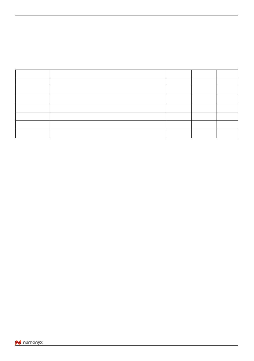
Table 11. Absolute Maximum Ratings
Symbol
Parameter
Min
Max
Unit
TBIAS
Temperature Under Bias
–50
125
°C
TSTG
Storage Temperature
–65
150
°C
TLEAD
Lead Temperature during Soldering
(1)
°C
VIO
Input or Output Voltage (2,3)
–0.6
VCC +0.6
V
VCC
Supply Voltage
–0.6
4
V
VID
Identification Voltage
–0.6
13.5
V
VPP(4)
Program Voltage
–0.6
13.5
V
Note: 1. Compliant with the JEDEC Std J-STD-020B (for small body, Sn-Pb or Pb assembly), and the European directive on Restrictions on
Hazardous Substances (RoHS) 2002/95/EU.
2. Minimum voltage may undershoot to –2V during transition and for less than 20ns during transitions.
3. Maximum voltage may overshoot to VCC +2V during transition and for less than 20ns during transitions.
4. VPP must not remain at 12V for more than a total of 80hrs.
23/51
Share Link: