M61040FP データシートの表示(PDF) - Renesas Electronics
部品番号
コンポーネント説明
メーカー
M61040FP Datasheet PDF : 25 Pages
| |||
M61040FP
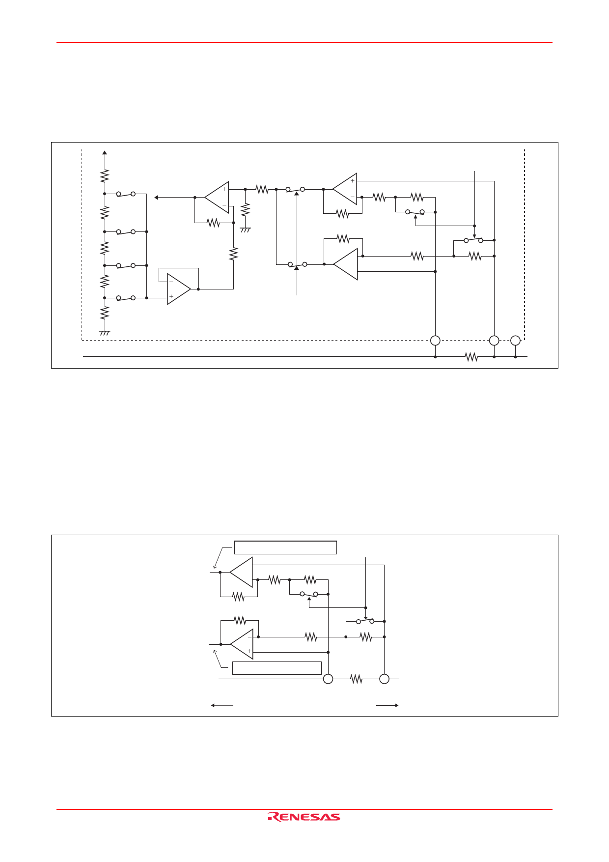
(2) Charge/discharge current detection circuit
The charge/discharge current detection circuit is shown in figure 4. This circuit is composed of offset voltage
adjustment circuit, buffer amplifier and resistor network.
The pre-amplifier amplifies the voltage of sense resistance to the voltage based on GND. The voltage gain can be
selected by microcomputer commands.
Buffer amplifier does an impedance translation between input and output.
Vreg = 5.2 V
To Multiplexer
circuit
AMP3
+
R
−
R
AMP2
+
−
RC1
Charge current
Monitor
RC3
RC2
From Serial to Parallel
conversion circuit
R
R
AMP4
Offset voltage
Adjustment circuit
RD1
−
+
Discharge current
Monitor
RD2
AMP1
From Serial to Parallel
conversion circuit
RD3
VIN11
12
VIN10
11
Rsence
GND
10
Figure 4 Charge/Discharge Current Detection Circuit
The offset voltage can be compensated by adjustment circuit.
The function in detecting discharge current is shown in figure 5. The differential voltage of sense resistor is input to
+ (plus) terminal of AMP 1 when discharge current is flowing in sense resistor. Selecting high voltage gain by
microcomputer's command is capable of monitoring very little discharge current accurately.
The differential voltage of sense resistor is input to – (minus) terminal of AMP 2 when charge current is flowing in
sense resistor. The methods of detecting in charging are the same as in discharging except that AMP2 reverses input
voltage before outputting.
Note: Regard 500 µs as the standard of settling time by voltage change in this block.
Vb = Idis • Rsens • Gain
+
AMP2
−
RC1
RC2
RC3
From I/F circuit
RD1 −
AMP+1
RD2
RD3
Va = Idis • Rsens • Gain
12
VIN11
Rsence
11
VIN10
Charge current Icha Discharge current Idis
Figure 5 Charge/Discharge Current Detection
REJ03F0237-0200 Rev.2.00 Mar 18, 2008
Page 12 of 24
Share Link: 