S3C821A データシートの表示(PDF) - Samsung
部品番号
コンポーネント説明
メーカー
S3C821A Datasheet PDF : 33 Pages
| |||
S3C821A/P821A
PRODUCT OVERVIEW
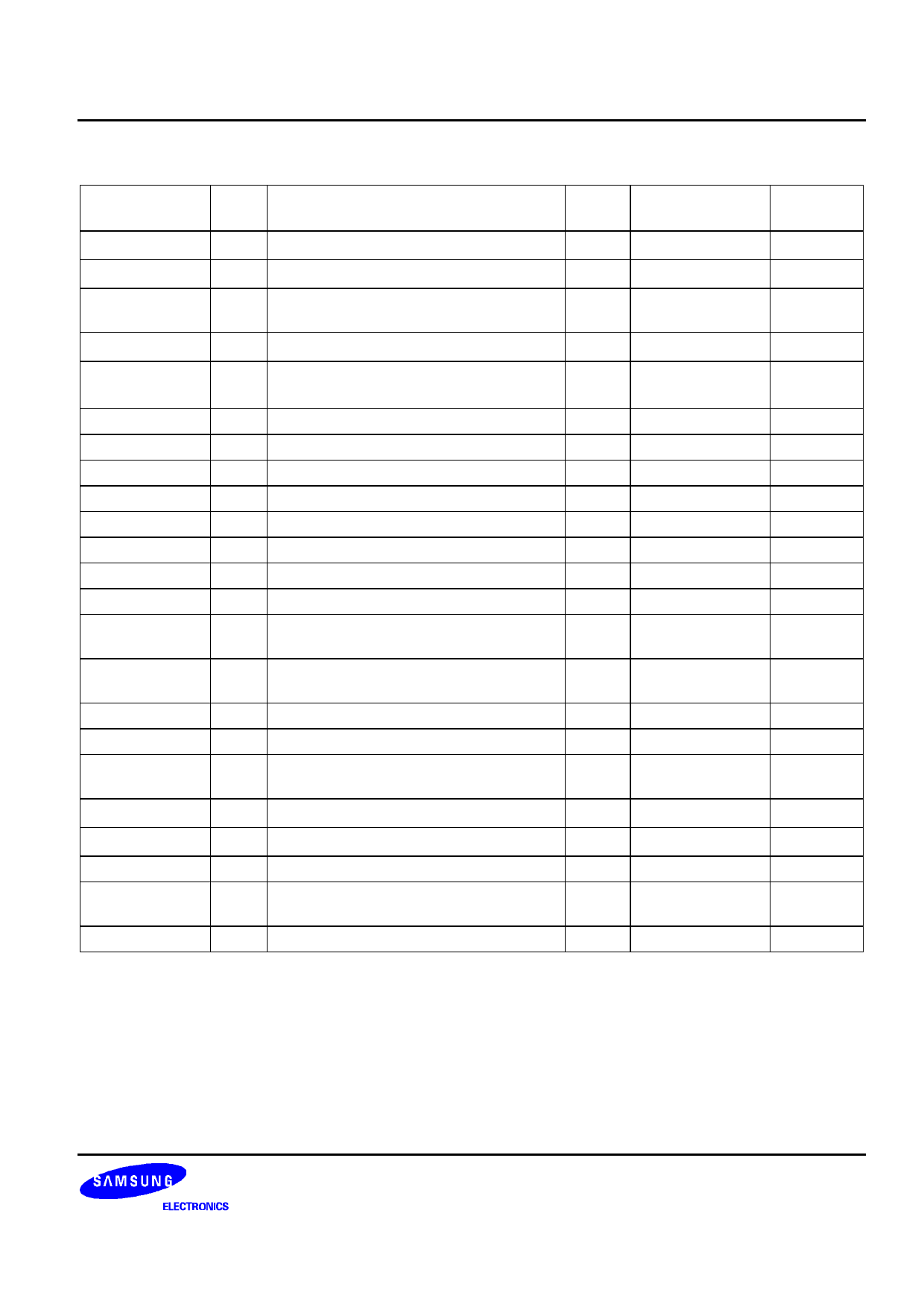
Table 1-1. S3C821A Pin Descriptions (Continued)
Pin
Names
VSS1, VDD1
XOUT, XIN
TEST
XTIN, XTOUT
RESET
INT0–INT3
T0CK
T1CK
TA
TB
T0
T0PWM
T0CAP
ADC0–ADC3
AVREF, AVSS
INT4–INT11
BUZ
SCK, SI, SO
VLC1
VSS2, VDD2
COM0–COM3
SEG0–SEG3
(COM4–COM7)
SEG4–SEG15
Pin
Type
Pin
Description
Circuit
Type
– Power input pins for internal power block –
– Main oscillator pins
–
– Chip test input pin
–
Hold GND when the device is operating
– Sub oscillator pins for sub-system clock
–
I RESET signal input pin. Schmitt trigger
input with internal pull-up resistor.
I/O External interrupts input with noise filter.
I/O 8Bit Timer 0 external clock input.
I/O Timer 1/A external clock input.
I/O Timer 1/A clock output
I/O Timer B clock output
I/O Timer 0 clock output
I/O Timer 0 PWM output
I/O Timer 0 capture input
I/O Analog input pins for A/D converts
module
– A/D converter reference voltage and
ground
I/O External interrupts input with noise filter.
I/O Buzzer signal output
I/O Serial clock, serial data input, serial data
output
– LCD bias voltage input pins
B
D-4
D-4
D-4
D-4
D-4
D-4
D-4
D-4
F-16
–
E-4
D-4
D-4
–
– Power input pins for external power block –
O LCD Common signal output
H-30
O LCD Common or Segment signal output H-31
O LCD segment signal output
H-29
Pin
Numbers (note)
10, 11 (12, 13)
12, 13 (14, 15)
14 (16)
15, 16 (17,18)
17 (19)
20–23 (22–25)
20 (22)
21 (23)
22 (24)
23 (25)
33 (35)
33 (35)
33 (35)
25–28 (27–30)
24, 29 (26, 31)
34–41 (36–43)
45 (47)
42–44 (44–46)
49 (51)
50, 51 (52, 53)
52–55 (54–57)
56–59 (58–61)
60–71 (62–73)
NOTE: Parentheses indicate pin number for 80-QFP package.
Share
Pins
–
–
–
–
–
P2.4–P2.7
P2.4
P2.5
P2.6
P2.7
P3.7
P3.7
P3.7
P3.0–P3.3
–
P4.0–P4.7
P5.3
P5.0–P5.2
–
–
–
–
–
1-7
Share Link: 