T80C251TB データシートの表示(PDF) - Intel
部品番号
コンポーネント説明
メーカー
T80C251TB Datasheet PDF : 36 Pages
| |||
8xC251TB/TQ HIGH-PERFORMANCE CHMOS MICROCONTROLLER
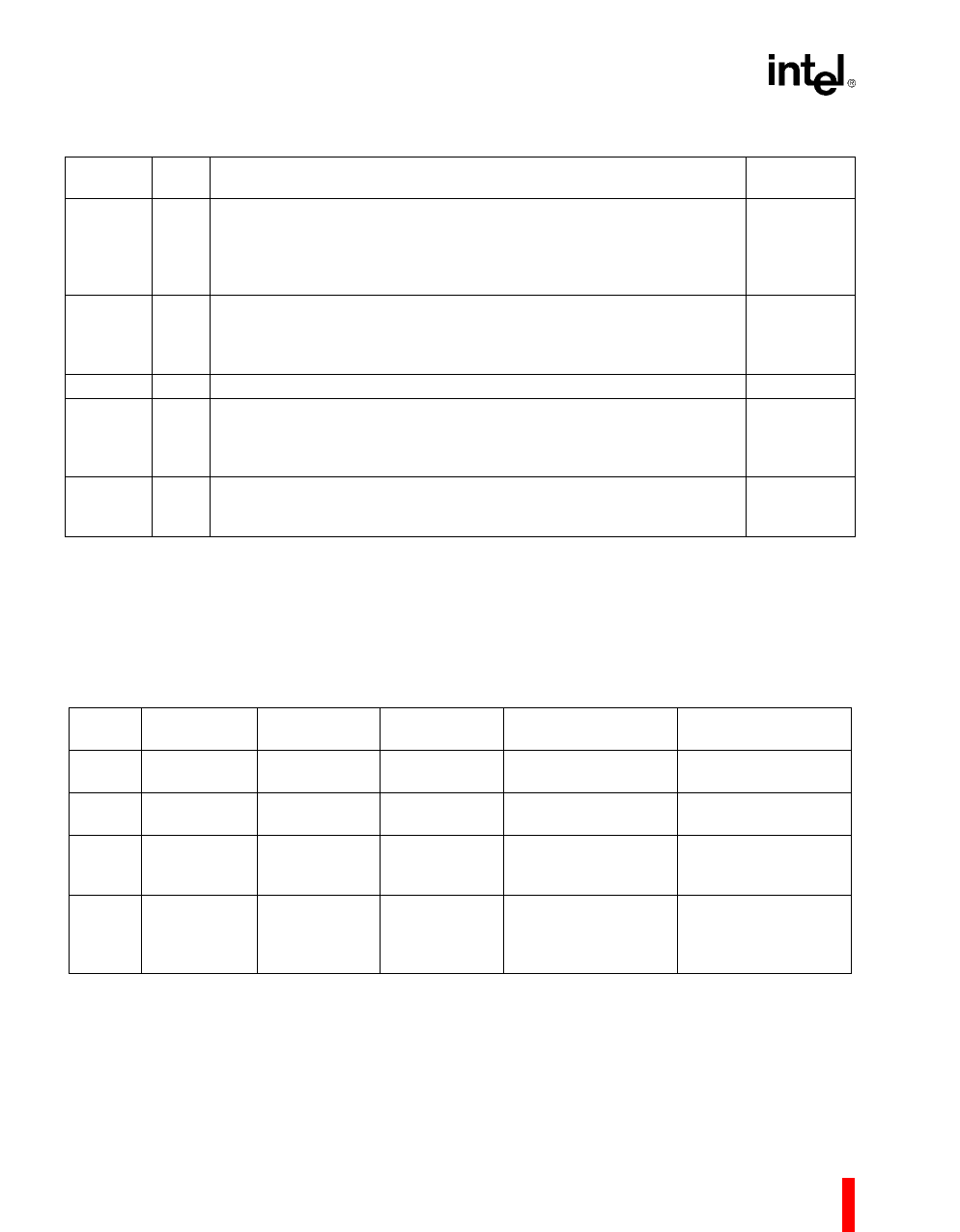
Table 6. Signal Descriptions (Sheet 3 of 3)
Signal
Name
Type
Description
Alternate
Function
WAIT#
I Real-time Wait State Input. The real-time WAIT# input is enabled by
P1.6/CEX3
writing a logical ‘1’ to the WCON.0 (RTWE) bit at S:A7H. During bus
cycles, the external memory system can signal ‘system ready’ to the
microcontroller in real time by controlling the WAIT# input signal on the
port 1.6 input.
WCLK
O Wait Clock Output. The real-time WCLK output is driven at port 1.7
P1.7/CEX4/
(WCLK) by writing a logical ‘1’ to the WCON.1 (RTWCE) bit at S:A7H. A17
When enabled, the WCLK output produces a square wave signal with a
period of one-half the oscillator frequency.
WR#
O Write. Write signal output to external memory.
P3.6
XTAL1
I Input to the On-chip, Inverting, Oscillator Amplifier. To use the
—
internal oscillator, a crystal/resonator circuit is connected to this pin. If an
external oscillator is used, its output is connected to this pin. XTAL1 is the
clock source for internal timing.
XTAL2
O Output of the On-chip, Inverting, Oscillator Amplifier. To use the
—
internal oscillator, a crystal/resonator circuit is connected to this pin. If an
external oscillator is used, leave XTAL2 unconnected.
NOTE:
The descriptions of A15:8/P2.7:0 and AD7:0/P0.7:0 are for the nonpage-mode chip configuration (compatible with 44-pin
PLCC and 40-pin DIP MCS 51 microcontrollers). If the chip is configured for page-mode operation, port 0 carries the lower
address bits (A7:0), and port 2 carries the upper address bits (A15:8) and the data (D7:0).
RD1:0
00
P1.7/CEX/
A17/WCLK
A17
0 1 P1.7/CEX4/
WCLK
1 0 P1.7/CEX4/
WCLK
1 1 P1.7/CEX4/
WCLK
Table 7. Memory Signal Selections (RD1:0)
P3.7/RD#/A16
PSEN#
WR#
A16
A16
P3.7 only
Asserted for all
addresses
Asserted for all
addresses
Asserted for all
addresses
Asserted for writes to
all memory locations
Asserted for writes to
all memory locations
Asserted for writes to
all memory locations
RD# asserted
for addresses
≤ 7F:FFFFH
Asserted for
≥ 80:0000H
Asserted only for
writes to MCS 51
microcontroller data
memory locations.
Features
256-Kbyte external
memory
128-Kbyte external
memory
64-Kbyte external
memory. One
additional port pin.
64-Kbyte external
memory. Compatible
with MCS 51 micro-
controllers.
10
Share Link: 