DS3510T データシートの表示(PDF) - Maxim Integrated
部品番号
コンポーネント説明
メーカー
DS3510T Datasheet PDF : 17 Pages
| |||
I2C Gamma and VCOM Buffer with EEPROM
Detailed Description
The DS3510 operates in one of three modes which
determine how the VCOM and gamma DACs are con-
trolled/updated. The first two modes allow “banked”
control of the 10 gamma channels and 1 VCOM chan-
nel. Depending on the mode, one of four banks (in
EEPROM) can be selected using either the S0/S1 pins
or using the SOFT S0/S1 bits in the Soft S0/S1 register.
Once a bank is selected, the LD pin can then be used
to simultaneously update each channel’s DAC output.
The third and final mode is not banked. It allows I2C
control of each channel’s Latch A register which is
SRAM (volatile), allowing quick and unlimited updates.
In this mode, the LD pin can also be used to simultane-
ously update each channel’s DAC output. A detailed
description of the three modes as well as additional
features of the DS3510 follows.
Mode Selection
The DS3510 mode of operation is determined by 2 bits
located in the Control register (60h), which is non-
volatile (NV) (EEPROM). In particular, the mode is
determined by the MODE0 bit (CR.0) and the MODE1
bit (CR.1). Table 1 illustrates how the 2 control bits are
used to select the operating mode. When shipped from
the factory, the DS3510 is programmed with both
MODE bits set to zero.
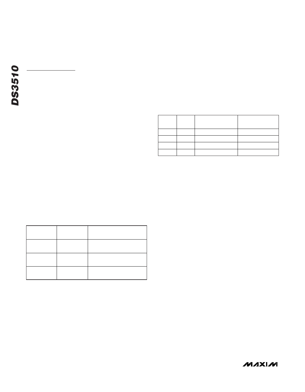
Table 1. DS3510 Operating Modes
MODE1 BIT
(CR.1)
0
0
1
MODE0 BIT
(CR.0)
MODE
S0/S1 Pin-Controlled Bank
0
Updating (Factory Default)
S0/S1 Bit-Controlled Bank
1
Updating
I2C Individual Channel
X
Control
S0/S1 Pin-Controlled Bank Updating Mode
As shown in the block diagram, each channel contains
4 bytes of EEPROM, which are used to implement the
“banking” functionality. Each “bank” contains unique
DAC settings for each channel. When the DS3510 is
configured in this operating mode, the desired bank is
selected using the S0 and S1 pins as shown in Table 2
where 0 is ground and 1 is VCC. For example, if S0 and
S1 are both connected to ground, then the first bank
(Bank A) is selected. Once a bank is selected, the tim-
ing of the DAC update depends on the state of LD pin.
When LD is high, Latch B functions as a flow-through
latch, so the amplifier will respond asynchronously to
changes in the state of S0/S1 to meet the tSEL specifi-
cation. Conversely, when LD is low, Latch B functions
as a latch, holding its previous data. A low-to-high tran-
sition on LD allows the Latch B input data to flow
through and update the DACs with the EEPROM bank
selected by S0/S1. A high-to-low transition on LD latch-
es the selected DAC data into Latch B.
Table 2. DS3510 Bank Selection Table
S1
S0
0
0
0
1
1
0
1
1
VCOM
CHANNEL
VCOM Bank A
VCOM Bank B
VCOM Bank C
VCOM Bank D
GAMMA
CHANNELS
GM1–10 Bank A
GM1–10 Bank B
GM1–10 Bank C
GM1–10 Bank D
SOFT S0/S1 (Bit) Controlled Bank
Updating Mode
This mode also features “banked” operation with the
only difference being how the desired bank is selected.
In particular, the bank is selected using the SOFT S0
(bit 0) and SOFT S1 (bit 1) bits contained in the Soft
S0/S1 register (50h). The S0 and S1 pins are ignored in
this mode. Table 2 illustrates the relationship between
the bit settings and the selected bank. For example, if
both bits, S0 and S1, are written to zero, then the first
bank (Bank A) is selected. Once a bank is selected, the
timing of the DAC update depends on the state of the
LD pin. When LD is high, Latch B functions as a flow-
through latch, so the amplifier will respond asynchro-
nously to changes in the state of the S0/S1 bits. These
are changed by an I2C write. Conversely, when LD is
low, Latch B functions as a latch, holding its previous
data. A low-to-high transition on LD allows the Latch B
input data to flow through and update the DACs with
the EEPROM bank selected by the S0/S1 bits. A high-
to-low transition on LD latches the selected DAC data
into Latch B.
Since the Soft S0/S1 register is SRAM, subsequent
power-ups result in the SOFT S0 and SOFT S1 bits
being cleared to 0 and, hence, powering up to Bank A.
I2C Individual Channel Control Mode
In this mode the I2C master writes directly to individual
channel Latch A registers to update a single DAC (i.e.,
not banked). The Latch A registers are SRAM and not
EEPROM. This allows an unlimited number of write
cycles as well as quicker write times since tW only
applies to EEPROM writes. As shown in the Memory
Map, the Latch A registers for each channel are
accessed through memory addresses 00–0Ah. Then,
10 ______________________________________________________________________________________
Share Link: 