CS7666-KQ データシートの表示(PDF) - Cirrus Logic
部品番号
コンポーネント説明
メーカー
CS7666-KQ Datasheet PDF : 42 Pages
| |||
CS7666
board are tied to the secondary I2C port of the
CS7666. WRITE and READ packets only are de-
fined in four-byte mode. Independent address set
operations to slave devices on the secondary I2C
bus is not allowed in four-byte mode. Four-byte
mode is active when the 4BYTEMODE pin (pin 1)
is logic high.
Write Operations in Four-Byte mode
All WRITE operations from an external controller,
through the CS7666, to any slave device must use
the four-byte mode; this includes writing to the
CS7666 itself. The external controller sends a four-
byte WRITE command to the CS7666 which ini-
tiates a WRITE operation to the destination slave
device and sets the I2CBUSY bit in the status reg-
ister (01h). The I2CBUSY bit is cleared when the
write operation on the secondary bus is complete.
The External controller can poll the status register
to check if the CS7666 has completed the com-
mand.
The CS7666 has a one command buffer which al-
lows the external controller to queue one additional
command while the current command is still being
executed. If more than one command is sent before
the I2CBUSY bit is cleared, the CS7666 saves only
the last command and executes it after the current
one is completed. Commands that involve writing
or reading only to CS7666 registers are not put in
the queue but are executed immediately without af-
fecting any transactions occurring on the master
I2C interface.
Any attempt by the external I2C controller to write
to the CS7666 registers while the CS7666 is busy
initializing from an external EEPROM will be ig-
nored. However, reads from the CS7666 are al-
lowed during this time.
If, during a READ or WRITE operation to a slave
device, the CS7666 fails to receive an acknowledge
bit the execution of the command is aborted and the
NODEV bit in the status register is set high. This
bit remains set unless it is explicitly cleared by
writing to it or a new command is written to
CS7666.
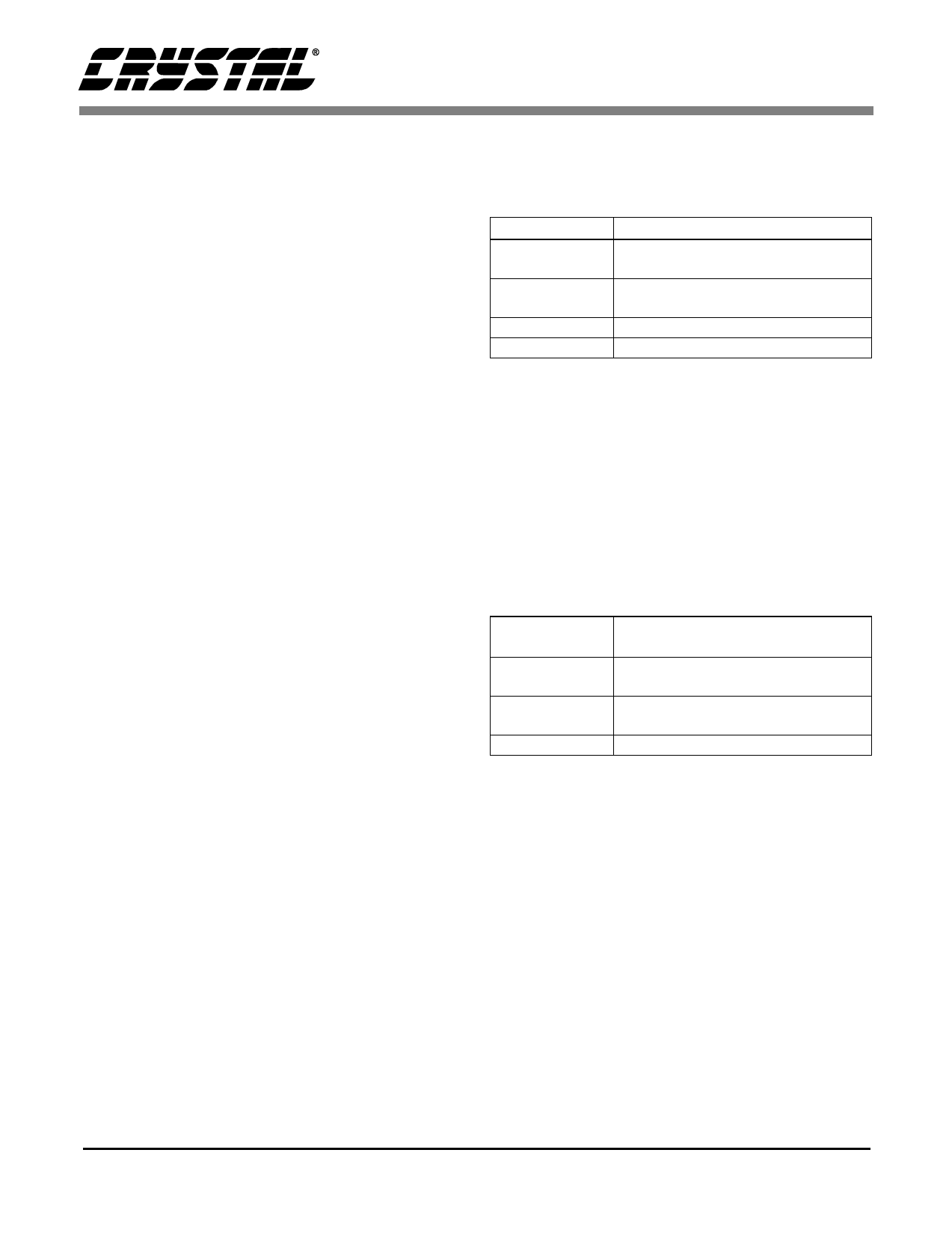
Byte Sequence WRITE Format Packet Detail
First Byte
Station Address of CS7666 with LSB
Set LOW
Second Byte Station Address of target slave
device with LSB Set LOW
Third Byte
Device Register Address (0..255)
Fourth Byte
Register Data (0..255)
Table 11. Four-byte WRITE Format Packet
Read Operations in Four-Byte Mode
The READ operation in four-byte mode first re-
quires a three-byte READ-TRIGGER packet to the
CS7666. The first byte is the station address of the
CS7666 with the LSB set LOW. The second byte is
the target slave device’s station address with the
LSB (data direction bit) set HIGH. The third byte is
the register address (0..255).
Byte Sequence READ-TRIGGER format Packet
Details
First Byte
CS7666 Station Address with LSB
Set LOW
Second Byte Target device Station Address with
LSB Set HIGH
Third Byte
Device Register Address (0..255)
Table 12. READ-TRIGGER packet in four-byte mode
The READ-TRIGGER packet initiates a READ
operation by the CS7666 from the target slave de-
vice on the secondary I2C bus. The status register
in the CS7666 may be checked to see if the read op-
eration has been completed. The I2CBUSY bit in
status register 01h is set to zero when the operation
is completed.
On completion of a read cycle from the target de-
vice, the CS7666 places the data read into the Slave
Data Hold register at address 19h. The external
controller can read this data through the primary
I2C port. This requires first performing an AD-
DRESS SET operation to set the address to 19h and
18
DS302PP1
Share Link: 