MAX6885 データシートの表示(PDF) - Maxim Integrated
部品番号
コンポーネント説明
メーカー
MAX6885 Datasheet PDF : 34 Pages
| |||
EEPROM-Programmable, Hex
Power-Supply Supervisory Circuits
Powering the MAX6884/MAX6885
The MAX6884/MAX6885 derive power from the voltage-
detector inputs: IN1–IN4 or through an externally sup-
plied VCC. A virtual diode-ORing scheme selects the
positive input that supplies power to the device (see the
Functional Diagram). The highest input voltage on
IN1–IN4 supplies power to the device. One of VIN1–VIN4
must be at least 2.7V to ensure proper operation.
Internal hysteresis ensures that the supply input that initially
powered the device continues to power the device when
multiple input voltages are within 50mV of each other.
VCC powers the analog circuitry and is the bypass con-
nection for the MAX6884/MAX6885 internal supply.
Bypass VCC to GND with a 1µF ceramic capacitor
installed as close to the device as possible. The internal
supply voltage, measured at VCC, equals the maximum
of IN1–IN4. If VCC is externally supplied, VCC must be at
least 200mV higher than any voltage applied to IN–IN4
and VCC must be brought up first. VCC always powers
the device when all IN_ are factory set as “ADJ.” Do not
use the internally generated VCC to provide power to
external circuitry. Externally supply power through VCC.
To externally supply power through VCC:
1) Apply a voltage to only one of VCC (2.7V to 5.5V) or
IN1–IN4 (2.7V to 5.8V).
2) Program the internal/external VCC Power EEPROM at
96h, Bit[5] = 1 (see Table 2).
3) Power down the device.
Subsequent power-ups and software reboots require an
externally supplied VCC to ensure the device is fully
operational.
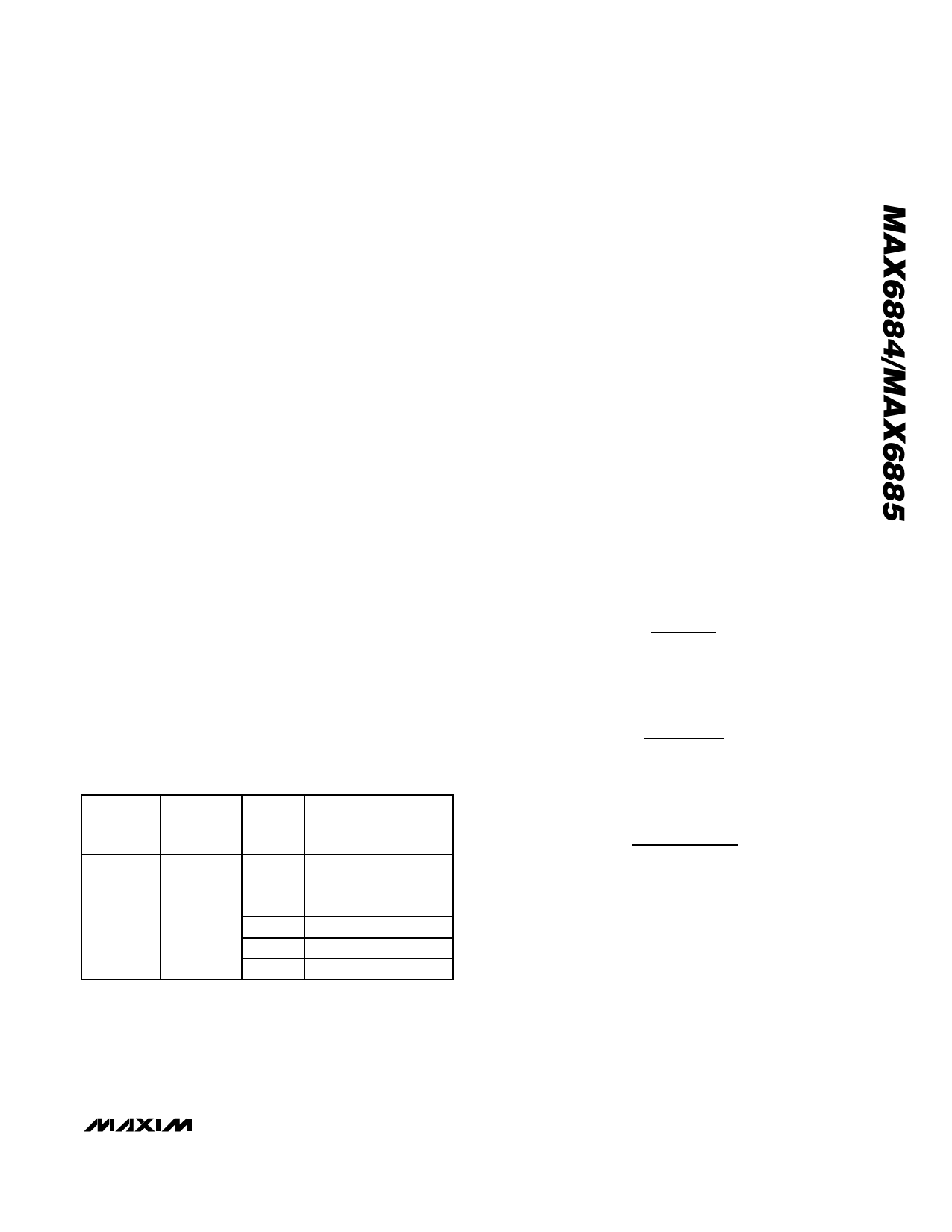
Table 2. Internal/External VCC
REGISTER
ADDRESS
EEPROM
MEMORY
ADDRESS
BIT
RANGE
DESCRIPTION
1 = VCC Powered
[5] 0 = IN1–IN4 or VCC
Powered
16h
96h
[2] Not Used
[4] Not Used
[6] Not Used
The MAX6884/MAX6885 also generate a digital supply
voltage (DBP) for the internal logic circuitry and the
EEPROM. Bypass DBP to GND with a 1µF ceramic
capacitor installed as close to the device as possible.
The nominal DBP output voltage is 2.55V. Do not use
DBP to provide power to external circuitry.
ADC (MAX6884 Only)
An internal 10-bit ADC (MAX6884 only) converts volt-
ages at IN1–IN4, AUXIN, and VCC through a multiplexer
that automatically sequences through all inputs every
200ms. Registers 18h to 27h store the ADC data (see
Table 3). Read the ADC data from the MAX6884 with
the serial interface. The ADC has no effect on program-
mable outputs RESET, UV/OV, or WDO.
Inputs
The MAX6884/MAX6885 offer the following inputs: volt-
age-detector inputs IN1–IN4, auxiliary input AUXIN
(MAX6884 only), manual reset input MR, margin input
MARGIN, and reference input REFIN (MAX6884 only).
IN1–IN6
The MAX6884/MAX6885 offer six voltage-detector inputs:
IN1–IN6. Each voltage-detector input offers a program-
mable primary undervoltage threshold and a secondary
undervoltage/overvoltage threshold. Program thresholds
from 0.5V to 3.05V in 10mV increments, 1.0V to 5.8V in
20mV increments, or from 0.1667V to 1.0167V in 3.3mV
increments. Use the following equations to program
thresholds in the appropriate registers:
X = VTH − 1V
0.02V
for 1V to 5.8V range in 20mV increments (program bits
R0Fh[5:0]).
X = VTH − 0.5V
0.01V
for 0.5V to 3.05V range in 10mV increments (program
bits R0Fh[5:0]).
X = VTH − 0.1667V
0.0033V
for 0.1667V to 1.0167V in 3.3mV increments (see the
External Voltage-Divider section).
where VTH is the desired threshold voltage and X is the
decimal code for the desired threshold (see Table 4). To
set a threshold for the 1V to 5.8V range, X must equal 240
or less. Set the secondary threshold for an undervoltage
or overvoltage threshold by programming bits R0Eh[5:0].
To achieve thresholds in between the 10mV and 20mV
steps or to monitor voltages higher than 5.8V, program a
voltage-detector input for high impedance through bits
R10h[5:0] and add a resister voltage-divider (see the
External Voltage-Divider section).
______________________________________________________________________________________ 13
Share Link: 