ICX252 データシートの表示(PDF) - Sony Semiconductor
部品番号
コンポーネント説明
メーカー
ICX252 Datasheet PDF : 46 Pages
| |||
CXD3406GA
Notes on Operation
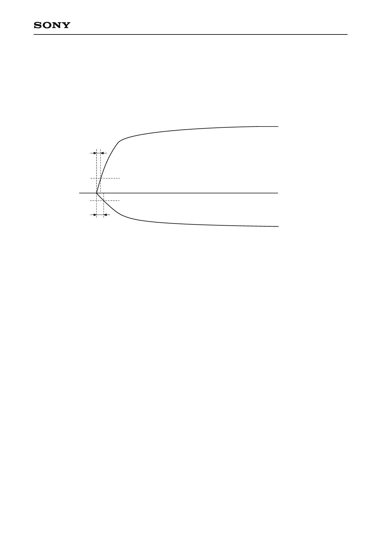
1. Be sure to start up the timing generator block VL and VH pin power supplies at the timing shown in the
figure below in order to prevent the SUB pin of the CCD image sensor from going to negative potential. In
addition, start up the timing generator block VDD1, VDD2, VDD3, VDD4 and VDD5 pin and CCD signal processor
block DVDD1, DVDD2, AVDD1, AVDD2, AVDD3, AVDD4 and AVDD5 pin power supplies at the same time either
before or at the same time as the VH pin power supply is started up.
15.0V
t1
20%
0V
20%
t2
t2 ≥ t1
–7.5V
2. Reset the timing generator block and CCD signal processor block during power-on. The timing generator
block is reset by inputting the reset signal to the RST pin. The CCD signal processor block is reset by
initializing the serial data.
3. Separate the timing generator block VDD1, VDD2, VDD3, VDD4 and VDD5 pins from the CCD signal processor
block DVDD1, DVDD2, AVDD1, AVDD2, AVDD3, AVDD4 and AVDD5 pins.
Also, the ADC output driver stage is connected to the dedicated power supply pin DVDD1. Separating this
pin from other power supplies is recommended to avoid affecting the internal analog circuits.
4. The difference in potential between the timing generator block VDD4 pin supply voltage 3 VDDc and the CCD
signal processor block DVDD1, DVDD2, AVDD1, AVDD2, AVDD3, AVDD4 and AVDD5 pin supply voltages 1 VDDe,
2 VDDf and 3 VDDg should be 0.1V or less.
5. The timing generator block and CCD signal processor block ground pins should use a shared ground which
is connected outside the IC. When the set ground is divided into digital and analog blocks, connect the
timing generator block ground pins to the digital ground and the CCD signal processor block ground pins to
the analog ground. The difference in potential between the timing generator block VSS1, VSS2, VSS3, VSS4,
VSS5, VSS6 and VM and the CCD signal processor block DVSS1, DVSS2, DVSS3, AVSS1, AVSS2, AVSS3, AVSS4,
AVSS5 and AVSS6 should be 0.1V or less.
6. Do not perform serial communication with the CCD signal processor block during the effective image
period, as this may cause the picture quality to deteriorate. In addition, using SCK2, SSI2 and SEN2, which
are used by the CCD signal processor block, use of the dedicated ports is recommended. When using
these pins as shared ports with the timing generator block or other ICs, be sure to thoroughly confirm the
effects on picture quality before use.
– 45 –
Share Link: 