87C196LA データシートの表示(PDF) - Intel
部品番号
コンポーネント説明
メーカー
87C196LA Datasheet PDF : 21 Pages
| |||
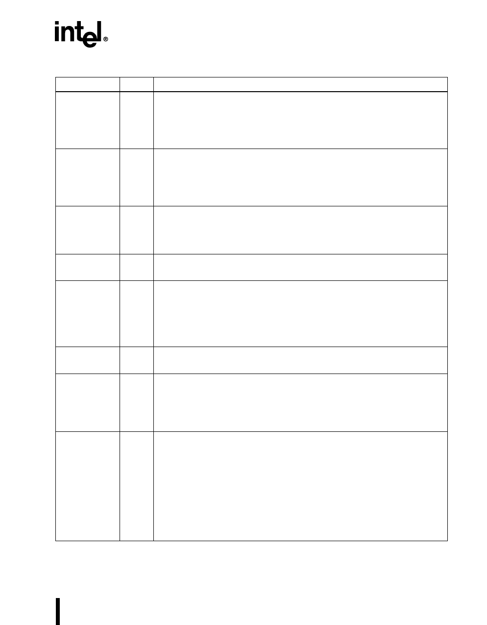
Name
T2CLK
T2DIR
TXD
VCC
VPP
VREF
VSS, VSS1
WR#
AUTOMOTIVE — 87C196LA
Type
I
I
O
PWR
PWR
PWR
GND
O
Table 4. Signal Descriptions (Continued)
Description
Timer 2 External Clock
External clock for timer 2. Timer 2 increments (or decrements) on both rising
and falling edges of T2CLK. It is also used in conjunction with T2DIR for
quadrature counting mode.
T2CLK shares a package pin with P1.0 and EPA0.
Timer 2 External Direction
External direction (up/down) for timer 2. Timer 2 increments when T2DIR is high
and decrements when it is low. It is also used in conjunction with T2CLK for
quadrature counting mode.
T2DIR shares a package pin with P1.2 and EPA2.
Transmit Serial Data
In serial I/O modes 1, 2, and 3, TXD transmits serial port output data. In mode
0, it is the serial clock output.
TXD shares a package pin with P2.0 and PVER.
Digital Supply Voltage
Connect each VCC pin to the digital supply voltage.
Programming Voltage
VPP causes the device to exit powerdown mode when it is driven low for at least
50 ns. Use this method to exit powerdown only when using an external clock
source because it enables the internal phase clocks, but not the internal
oscillator.
If you do not plan to use the powerdown feature, connect VPP to VCC.
Reference Voltage for the A/D Converter
This pin supplies operating voltage to the A/D converter.
Digital Circuit Ground
These pins supply ground for the digital circuitry. Connect each VSS and VSS1 pin
to ground through the lowest possible impedance path. VSS pins are connected
to the core ground region of the microcontroller, while VSS1 pins are connected
to the port ground region. (ANGND is connected to the analog ground region.)
Separating the ground regions provides noise isolation.
Write†
This active-low output indicates that an external write is occurring. This signal is
asserted only during external memory writes.
Forcing WR# high while RESET# is low causes the device to enter PLL-bypass
mode. When the device is in PLL-bypass mode, the internal phase clocks
operate at one-half the frequency of the frequency on XTAL1.
WR# shares a package pin with P5.2, WRL#, and PLLEN.
† When this pin is configured as a special-function signal (P5_MODE.2 = 1), the
chip configuration register 0 (CCR0) determines whether it functions as WR#
or WRL#. CCR0.2 = 1 selects WR#; CCR0.2 = 0 selects WRL#.
PRODUCT PREVIEW
13
Share Link: 