AD1582(RevM) データシートの表示(PDF) - Analog Devices
部品番号
コンポーネント説明
メーカー
AD1582 Datasheet PDF : 17 Pages
| |||
AD1582/AD1583/AD1584/AD1585
100
1µF CAP
10
AD1585
AD1582
1
10µV
100
90
10
0%
Data Sheet
1s
0.1
10
100
1k
10k
100k
1M
FREQUENCY (Hz)
Figure 17. Output Impedance vs. Frequency
10V
10kΩ
×1
5V ± 100mV
±200mV 10kΩ
0.22µF
DUT VOUT
0.22µF
Figure 18. Ripple Rejection Test Circuit
100
90
80
70
AD1582
60
50
AD1585
40
30
20
10
0
1
10
100
1k
10k
100k
1M
FREQUENCY (Hz)
Figure 19. Ripple Rejection vs. Frequency
NOISE PERFORMANCE AND REDUCTION
The noise generated by the AD1582/AD1583/AD1584/AD1585 is
typically less than 70 μV p-p over the 0.1 Hz to 10 Hz frequency
band. Figure 20 shows the 0.1 Hz to 10 Hz noise of a typical
AD1582/AD1583/AD1584/AD1585. The noise measurement is
made with a high gain band-pass filter. Noise in a 10 Hz to
10 kHz region is approximately 50 μV rms. Figure 21 shows the
broadband noise of a typical AD1582/AD1583/AD1584/
AD1585. If further noise reduction is desired, add a 1-pole,
low-pass filter between the output pin and ground. A time
constant of 0.2 ms has a −3 dB point at roughly 800 Hz and
reduces the high frequency noise to about 16 V rms. It should
be noted, however, that while additional filtering on the output
can improve the noise performance of the AD1582/AD1583/
AD1584/AD1585, the added output impedance can degrade the
ac performance of the references.
Figure 20. 10 Hz to 10 kHz Wideband Noise
100µV
100
90
10ms
10
0%
Figure 21. 1 Hz to 10 Hz Voltage Noise
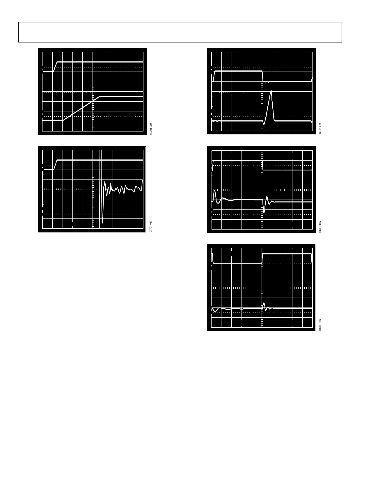
TURN-ON TIME
Many low power instrument manufacturers are concerned
with the turn-on characteristics of the components used in
their systems. Fast turn-on components often enable the end
user to save power by keeping power off when not needed.
Turn-on settling time is defined as the time required, after the
application of power (cold start), for the output voltage to reach
its final value within a specified error. The two major factors
affecting this are the active circuit settling time and the time
required for the thermal gradients on the chip to stabilize.
Figure 22 shows the turn-on settling and transient response test
circuit. Figure 23 shows the turn-on characteristics of the
AD1582/AD1583/ AD1584/AD1585. These characteristics are
generated from cold-start operation and represent the true
turn-on waveform after power-up. Figure 24 shows the fine
settling characteristics of the AD1582/AD1583/AD1584/
AD1585. Typically, the reference settles to within 0.1% of its
final value in about 100 μs.
The device can momentarily draw excessive supply current
when VSUPPLY is slightly below the minimum specified level.
Power supply resistance must be low enough to ensure reliable
turn-on. Fast power supply edges minimize this effect.
Rev. M | Page 14 of 17
Share Link: 