FM1608-120-PG データシートの表示(PDF) - Ramtron International Corporation
部品番号
コンポーネント説明
メーカー
FM1608-120-PG Datasheet PDF : 11 Pages
| |||
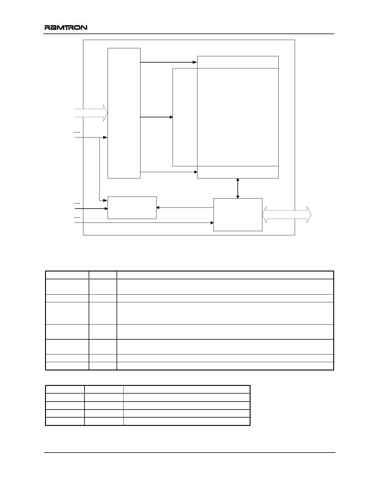
A10-A12
Block Decoder
FM1608
A0-A12
CE
Address
Latch
A0-A7
Row
Decoder
8,192 x 8 FRAM Array
A8-A9
Column Decoder
WE
Control
Logic
OE
I/O Latch
Bus Driver
DQ0-7
Figure 1. Block Diagram
Pin Description
Pin Name
A0-A12
DQ0-7
/CE
/OE
/WE
VDD
VSS
I/O
Input
I/O
Input
Input
Input
Supply
Supply
Pin Description
Address: The 13 address inputs select one of 8,192 bytes in the FRAM array. The
address value will be latched on the falling edge of /CE.
Data: 8-bit bi-directional data bus for accessing the FRAM array.
Chip Enable: /CE selects the device when low. Asserting /CE low causes the address
to be latched internally. Address changes that occur after /CE goes low will be
ignored until the next falling edge occurs.
Output Enable: Asserting /OE low causes the FM1608 to drive the data bus when
valid data is available. Deasserting /OE high causes the DQ pins to be tri-stated.
Write Enable: Asserting /WE low causes the FM1608 to write the contents of the
data bus to the address location latched by the falling edge of /CE.
Supply Voltage: 5V
Ground.
Functional Truth Table
/CE
/WE
H
X
↓
X
L
H
L
↓
Function
Standby/Precharge
Latch Address (and Begin Write if /WE=low)
Read
Write
Note: The /OE pin controls only the DQ output buffers.
Rev. 3.0
Nov. 2004
2 of 11
Share Link: 