935267010117 データシートの表示(PDF) - Philips Electronics
部品番号
コンポーネント説明
メーカー
935267010117 Datasheet PDF : 17 Pages
| |||
Philips Semiconductors
Frame Transfer CCD Image Sensor
Objective specification
FXA 1012
Application information
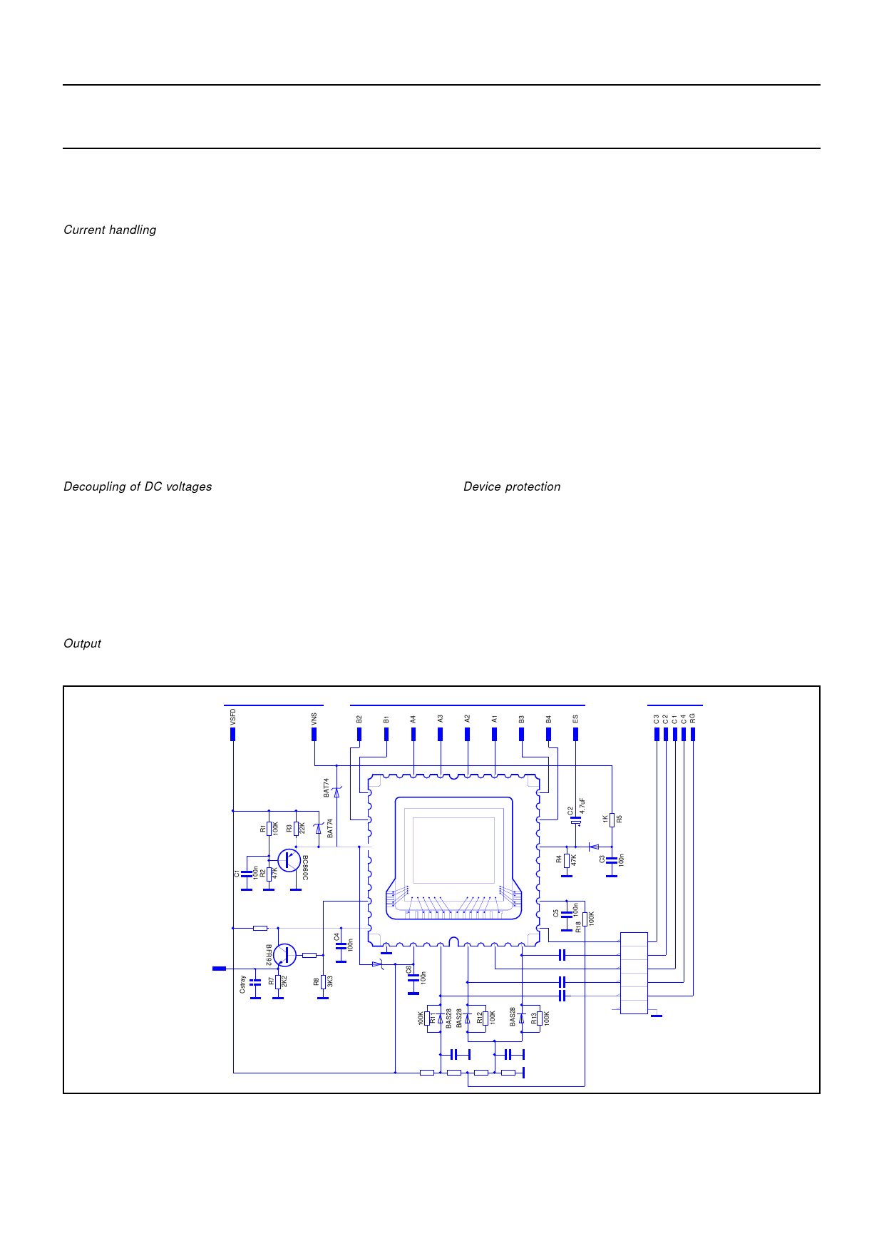
Current handling
One of the purposes of VPS is to drain the holes that are generated
during exposure of the sensor to light. Free electrons are either
transported to the VRD connection and, if excessive (from over-
exposure), free electrons are drained to VNS. No current should
flow into VPS. During overexposures a total current 0.5 to 1mA
through VPS may be expected. The PNP emitter follower in the circuit
diagram (figure 9) serves these current requirements.
VNS drains superfluous electrons as a result of overexposure. In
other words, it only sinks current. During overexposures a total current
of 0.5 to 1mA through VNS may be expected. The NPN emitter
follower in the circuit diagram meets these current requirements.
The clamp circuit, consisting of the diode and electrolytic capacitor,
enables the addition of a Charge Reset (CR) pulse on top of an
otherwise stable VNS voltage. To protect the CCD, the current
resulting from this pulse should be limited. This can be accomplished
by designing a pulse generator with a rather high output impedance.
a current source or more simply with a resistance to GND. In order
to prevent the output (which typically has an output impedance of
about 400 Ohm) from bandwidth limitation as a result of capacitive
loading, load the output with an emitter follower built from a high-
frequency transistor. Mount the base of this transistor as close as
possible to the sensor and keep the connection between the emitter
and the next stage short. The CCD output buffer can easily be
destroyed by ESD. By using this emitter follower, this danger is
suppressed; do NOT reintroduce this danger by measuring directly
on the output pin of the sensor with an oscilloscope probe. Instead,
measure on the output of the emitter follower. Slew rate limitation is
prevented by avoiding a too-small quiescent current in the emitter
follower; about 10mA should do the job. The collector of the emitter
follower should be decoupled properly to suppress the Miller effect
from the base-collector capacitance. A CCD output load resistor of
3.3 kΩ typically results in a bandwidth of 95MHz.
Decoupling of DC voltages
All DC voltages (not VNS, which has additional CR pulses as
described above) should be decoupled with a 100nF decoupling
capacitor. This capacitor must be mounted as close as possible to
the sensor pin. Further noise reduction (by bandwidth limiting) is
achieved by the resistors in the connections between the sensor
and its voltage supplies. The electrons building up the charge packets
that will reach the floating diffusion only add up to a small current,
which will flow through VRD. Therefore a large series resistor in the
VRD connection may be used.
Output
To limit the on-chip power dissipation, the output buffer is designed
with open source output. The output should therefore be loaded with
Device protection
The output buffer or VNS of the FXA 1012 is likely to be damaged if
VPS rises above SFD or RD at any time.This danger is most realistic
during power-on or power-off of the camera.
Never exceed the maximum output current. This may damage the
device permanently. The maximum output current should be limited
to 6mA. Be especially aware that the output buffers of these image
sensors are very sensitive to ESD damage.
Because of the fact that our CCDs are built on an n-substrate, we
are dealing with some parasitic NPN transistors. To avoid activation
of these transistors during switch-on and switch-off of the camera,
we recommend the application diagram of figure 9.
From CCD Supply
From V-Drivers
From PPG
CCD OUT
47E
R6
R9
100E
NC
A4
A3
A2
A1
NC
B1
B3
B2
B4
VPS
FXA 1012
VNS
NC
NC
BAS28
OUT
OG
SFD
SFS RD
RG
C4
BAT74
C3
C1
C2
C7 100n
C8 100n
C9 100n
H DRIVER
1
74ACT04
C10 100n
C11 100n
R14 R15 R16 R17
22K 100K 6K8 18K
Figure 9 - Application diagram to protect the FXA 1012
2000 January
12
Share Link: 