MAX4473EUA(1999) データシートの表示(PDF) - Maxim Integrated
部品番号
コンポーネント説明
メーカー
MAX4473EUA
(Rev.:1999)
(Rev.:1999)
Maxim Integrated

MAX4473EUA Datasheet PDF : 6 Pages
| |||
Low-Cost, Low-Voltage, PA Power Control
Amplifier for GSM Applications in 8-Pin µMAX
Pin Description
PIN NAME
FUNCTION
1
SR1
Inverting Input of Error Amplifier and Drain of V-to-I FET, Q1. Connect to supply side of current-sense resis-
tor, RSENSE, through gain resistor RG1.
2
SR2
Noninverting Input of Error Amplifier. Connect to load side of current-sense resistor, RSENSE, through gain
resistor RG2. Set RG2 equal to RG1.
Shutdown Input. Drive SHDN low to disable all amplifiers, pull OUT to GND, set the gate-to-source voltage
3
SHDN of the V-to-I FET (Q1) to 0, and reduce supply current to less than 1µA. Drive high or connect to VCC for nor-
mal operation.
4
PC
Power Control Input. Apply a voltage to PC to set a DC current through the sense resistor to control PA bias.
5
GND Ground
6
SR3
Inverting Input of V-to-I Converter and Source of V-to-I FET, Q1. Connect to ground through gain resistor
RG3.
7
OUT Output of Error Amplifier. Connect to gain control pin of power amplifier in bias control applications.
8
VCC +2.7V to +6.5V Voltage Supply Input. Bypass to ground with a 0.1µF capacitor.
Detailed Description
The MAX4473 is a voltage-controlled, unidirectional,
high-side current setting amplifier for applications
where accurate control of PA supply current is desired.
This device is intended for wireless TDMA based sys-
tems (GSM, DECT), where tight restrictions over the
PA’s transmit burst and output power require closed-
loop control over the PA’s output power. When used
with a PA, the MAX4473 functions as a voltage-con-
trolled constant current source, accurately setting PA
supply current by varying the gain of the PA. If you
know the output power versus supply current profile for
the PA, you can set the PA’s output power by control-
ling the amount of supply current delivered to the PA.
The MAX4473 is composed of an input buffer (A1), a
voltage-to-current converting amplifier (A2), and a rail-
to-rail output error amplifier (A3) (see Typical Operating
Circuit). External gain and sense resistors allow pro-
grammability for a wide range of applications.
In the Typical Operating Circuit, PA supply current
flows from the system supply, through the external cur-
rent sense resistor (RSENSE), to the PA. The rail-to-rail
outputs of the error amplifier, A3, adjust the gain of the
PA until the voltage drop across RSENSE equals the
voltage drop across external gain resistor, RG1. The
voltage drop across RG1 sets the voltage drop across
RSENSE, with a larger voltage drop resulting in more
current delivered to the PA. The voltage drop across
RG1 is set by A1, A2, and the V-to-I FET, Q1. A voltage
applied to the PC input of the input buffer is divided by
four by a resistor-divider network. A2 forces its inverting
input and the source of Q1 to VPC / 4, thus setting a
voltage across RG3. The resulting current through RG3
sets the current through RG1. This unique architecture
allows the supply current to be set independent of sup-
ply voltage. Set PA supply current according to the fol-
lowing equation:
ICCPA = ( VPC · RG1 ) / ( 4 · RSENSE · RG3 )
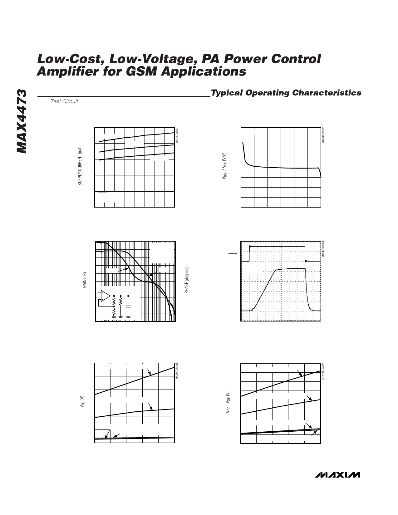
Shutdown Mode
When SHDN is a logic-level low (SHDN < 0.4V), ampli-
fiers A1, A2, and A3 are off, Q1 is turned off, and the
output of A3 is actively pulled to ground with an N-
channel FET. Supply current is reduced to less than
1µA in shutdown mode. Typical power-up time is 0.9µs
and typical power-down time is 0.3µs, using the
MAX4473 test circuit.
Applications Information
Gain Resistor Selection
(RG1, RG2, RG3)
For proper operation, do not make the value of external
gain resistors RG1 and RG2 larger than twice the value
of RG3. In most practical applications, choose RG1
smaller than RG3 to limit the voltage drop over RG1
and RSENSE. A large voltage drop over RSENSE sub-
stantially reduces the voltage applied to the PA, thus
reducing PA output power. Set RG2 equal to RG1 to
compensate for the input bias currents of A3.
Recommended values for RG3 are between 1kΩ and
10kΩ.
4 _______________________________________________________________________________________
Share Link: