LH168R データシートの表示(PDF) - Sharp Electronics
部品番号
コンポーネント説明
メーカー
LH168R Datasheet PDF : 19 Pages
| |||
LH168R
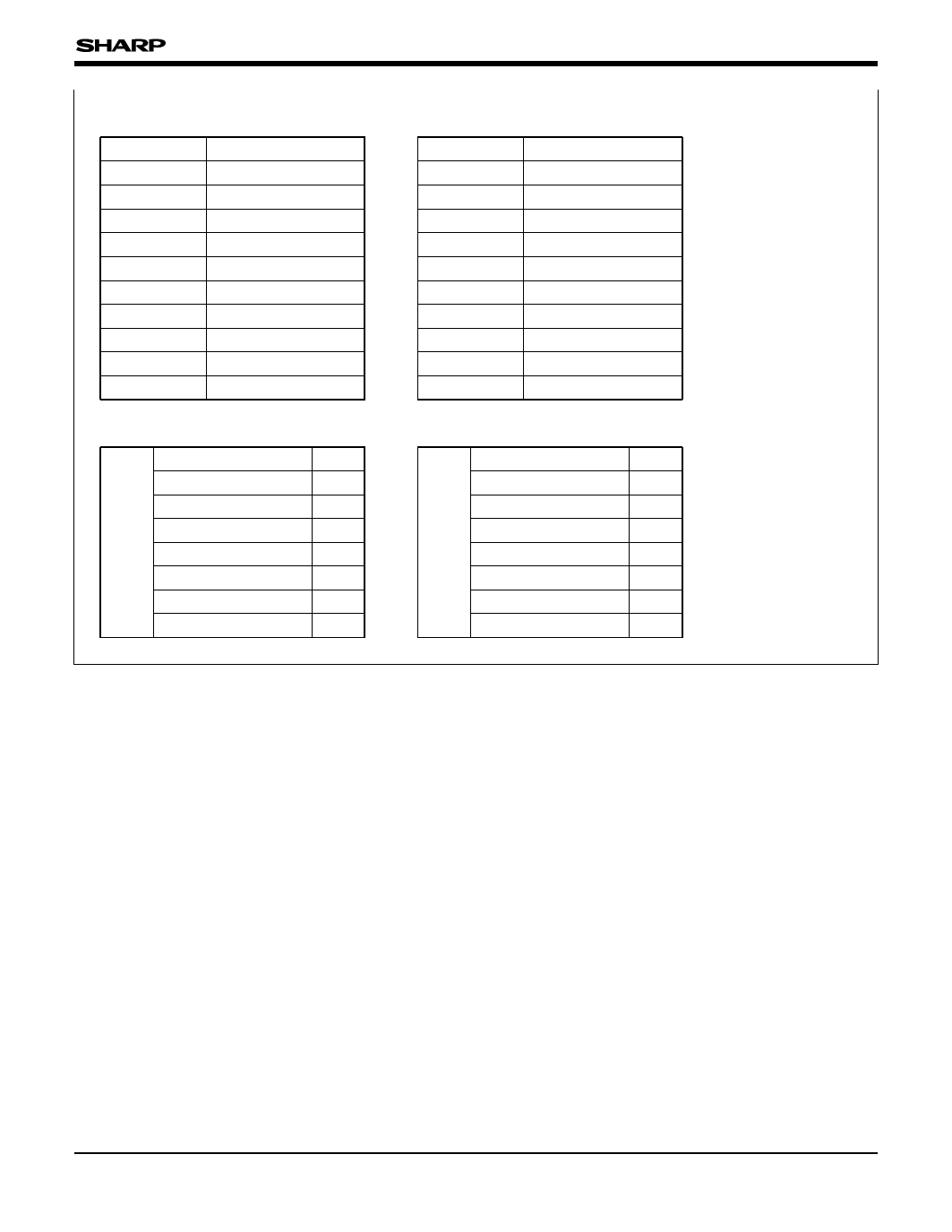
The following shows the ratio of ‹ correction resistance, when R0 equals 1.
R0
1.00
R83
0.99
R1
0.60
R82
0.45
R2
0.49
R81
0.36
R3
0.52
R80
0.33
R4
0.60
R9
1.00
R5
0.74
R10
0.74
R6
1.00
R11
0.60
R70
0.33
R12
0.52
R71
0.36
R13
0.49
R72
0.45
R14
0.60
R73
0.99
R15
1.00
The following shows the ratio of ‹ correction resistance of R73 and R83, when R730 equals 1.
R730
1.00
R837 (VL256 side)
2.35
R731
1.00
R836
0.87
R732
1.00
R835
0.87
R733
R73
R734
1.00
0.87
R834
R83
R833
0.87
1.00
R735
0.87
R832
1.00
R736
0.87
R831
1.00
R737 (VH256 side)
2.35
R830
1.00
PRECAUTIONS
Precautions when connecting or disconnecting
the power supply
This IC has some power supply pins, so it may be
permanently damaged by a high current which may
flow if voltage is supplied to the LCD drive power
supply while the logic system power supply is
floating. Therefore, when connecting the power
supply, observe the following sequence.
VCC / logic input / VLS, VH0-VH256, VL0-VL256
When disconnecting the power supply, follow the
reverse sequence.
Reference voltage input
The relation of the reference voltage input is shown
here.
VLS > VH0 ≥ VH32 ≥ π ≥ VH224 ≥ VH256 ≥ 0.5VLS
≥ VL256 ≥ VL224 ≥ π ≥ VL32 ≥ VL0 > GND
Maximum ratings
When connecting or disconnecting the power
supply, this IC must be used within the range of the
absolute maximum ratings.
Target output load
This IC is designed for a 200 pF output load
capacity. When using this IC for other than 200 pF
panels, confirm the device is having no problem
before using it.
12
Share Link: 