Q67120-C1026 データシートの表示(PDF) - Infineon Technologies
部品番号
コンポーネント説明
メーカー
Q67120-C1026 Datasheet PDF : 43 Pages
| |||
C511 / C513
Timer/ Counter 0 and 1
Timer/Counter 0 and 1 can be used in four operating modes as listed in table 7:
Table 7
Timer/Counter 0 and 1 operating modes
Mode Description
0 8-bit timer/counter with a
divide-by-32 prescaler
1 16-bit timer/counter
2 8-bit timer/counter with
8-bit auto-reload
3 Timer/counter 0 used as one
8-bit timer/counter and one
8-bit timer
Timer 1 stops
Gate
X
TMOD
C/T M1
X0
XX0
XX1
XX1
Input Clock
M0 internal external (max)
0
f / OSC 12 × 32
f / OSC 24 × 32
1
f / OSC 12
0
f / OSC 12
f / OSC 24
f / OSC 24
1
f / OSC 12
f / OSC 24
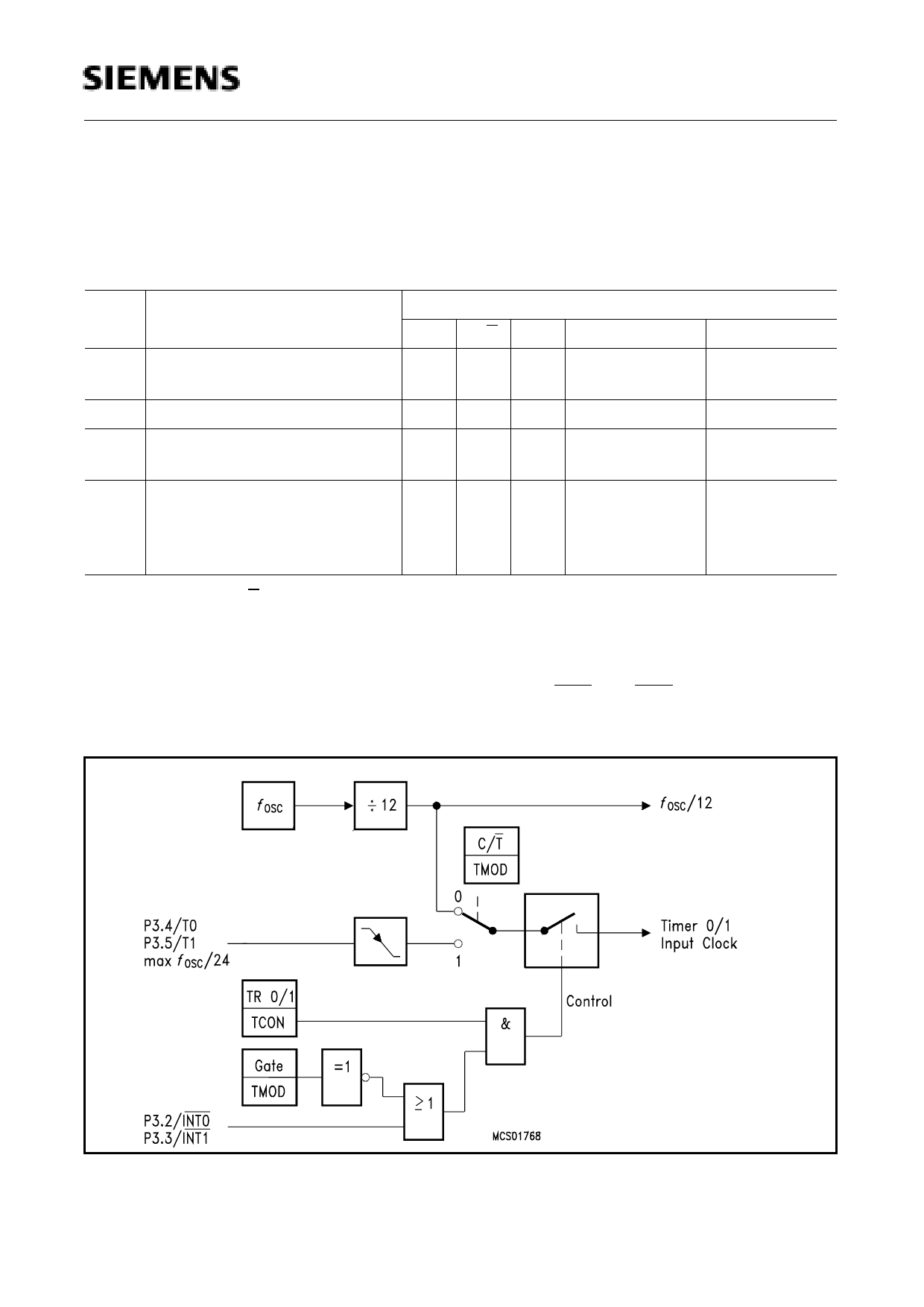
In “timer” function (C/T = ‘0’) the register is incremented every machine cycle. Therefore the count
rate is fOSC/12.
In “counter” function the register is incremented in response to a 1-to-0 transition at its
corresponding external input pin (P3.4/T0, P3.5/T1). Since it takes two machine cycles to detect a
falling edge the max. count rate is fOSC/24. External inputs INT0 and INT1 (P3.2, P3.3) can be
programmed to function as a gate to facilitate pulse width measurements. Figure 7 illustrates the
input clock logic.
Figure 7
Timer/Counter 0 and 1 Input Clock Logic
Semiconductor Group
21
Share Link: 