MB89610R データシートの表示(PDF) - Fujitsu
部品番号
コンポーネント説明
メーカー
MB89610R Datasheet PDF : 44 Pages
| |||
MB89610R Series
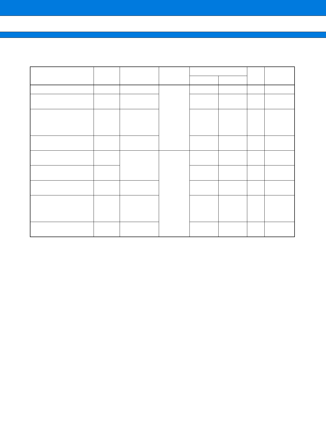
(9) Serial I/O Timing
Parameter
Symbol
(VCC = +5.0 V±10%, FC = 10 MHz, VSS = 0.0 V, TA = –40°C to +85°C)
Value
Pin
Condition
Unit Remarks
Min.
Max.
Serial clock cycle time tSCYC
SCK1, SCK2
2 tinst*
—
µs
SCK1 ↓ → SO1 time
SCK2 ↓ → SO2 time
tSLOV
SCK1, SO1
SCK2, SO2
–200
200
ns
SCK1 ↑ → valid SI1 hold
Internal
time
SCK2 ↑ → valid SI2 hold
tSHIX
SCK1, SI1
SCK2, SI2
shift clock
mode
1/2 tinst*
—
µs
time
Valid SI1 → SCK1 ↑
Valid SI2 → SCK2 ↑
tIVSH
SI1, SCK1
SI2, SCK2
1/2 tinst*
—
µs
Serial clock “H” pulse
width
tSHSL
Serial clock “L” pulse
width
tSLSH
SCK1, SCK2
1 tinst*
1 tinst*
—
µs
—
µs
SCK ↓ → SO1 time
SCK2 ↓ → SO2 time
tSLOV
SCK1, SO1
SCK2, SO2
External
shift clock
0
200
ns
SCK1 ↑ → valid SI1 hold
mode
time
SCK2 ↑ → valid SI2 hold
tSHIX
SCK1, SI1
SCK2, SI2
1/2 tinst*
—
µs
time
Valid SI1 → SCK1 ↑
Valid SI2 → SCK2 ↑
tIVSH
SI1, SCK1
SI2, SCK2
1/2 tinst*
—
µs
* : For information on tinst, see “(4) Instruction Cycle.”
30
Share Link: 