NID9N05ACL(2016) データシートの表示(PDF) - ON Semiconductor
部品番号
コンポーネント説明
メーカー
NID9N05ACL Datasheet PDF : 7 Pages
| |||
NID9N05ACL, NID9N05BCL
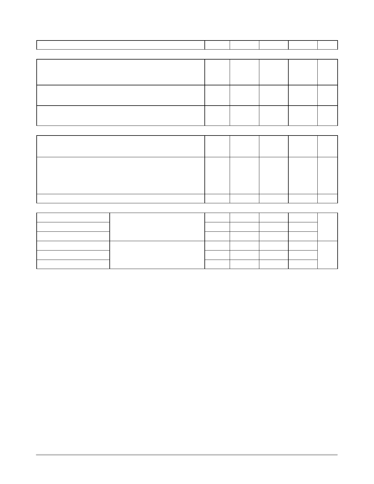
ELECTRICAL CHARACTERISTICS (TJ = 25°C unless otherwise noted)
Characteristic
Symbol
Min
Typ
Max
Unit
OFF CHARACTERISTICS
Drain−to−Source Breakdown Voltage (Note 3)
(VGS = 0 V, ID = 1.0 mA, TJ = 25°C)
(VGS = 0 V, ID = 1.0 mA, TJ = −40°C to 125°C)
Temperature Coefficient (Negative)
V(BR)DSS
52
55
59
V
50.8
54
59.5
V
−
−10
−
mV/°C
Zero Gate Voltage Drain Current
(VDS = 40 V, VGS = 0 V)
(VDS = 40 V, VGS = 0 V, TJ = 125°C)
Gate−Body Leakage Current
(VGS = ±8 V, VDS = 0 V)
(VGS = ±14 V, VDS = 0 V)
ON CHARACTERISTICS (Note 3)
IDSS
−
−
IGSS
−
−
mA
−
10
−
25
mA
−
±10
±22
−
Gate Threshold Voltage (Note 3)
(VDS = VGS, ID = 100 mA)
Threshold Temperature Coefficient (Negative)
VGS(th)
1.3
−
1.75
−4.5
2.5
V
−
mV/°C
Static Drain−to−Source On−Resistance (Note 3)
(VGS = 4.0 V, ID = 1.5 A)
(VGS = 3.5 V, ID = 0.6 A)
(VGS = 3.0 V, ID = 0.2 A)
(VGS = 12 V, ID = 9.0 A)
(VGS = 12 V, ID = 12 A)
RDS(on)
−
−
−
70
67
mW
153
181
175
364
−
1210
90
−
95
−
Forward Transconductance (Note 3) (VDS = 15 V, ID = 9.0 A)
DYNAMIC CHARACTERISTICS
gFS
−
24
−
Mhos
Input Capacitance
Ciss
−
Output Capacitance
(VDS = 40 V, VGS = 0 V, f = 10 kHz)
Coss
−
Transfer Capacitance
Crss
−
Input Capacitance
Ciss
−
Output Capacitance
(VDS = 25 V, VGS = 0 V, f = 10 kHz)
Coss
−
Transfer Capacitance
Crss
−
SWITCHING CHARACTERISTICS (Note 4)
155
250
pF
60
100
25
40
175
−
pF
70
−
30
−
Turn−On Delay Time
td(on)
−
130
200
ns
Rise Time
Turn−Off Delay Time
(VGS = 10 V, VDD = 40 V,
ID = 9.0 A, RG = 9.0 W)
tr
−
td(off)
−
500
1300
750
2000
Fall Time
tf
−
1150
1850
Turn−On Delay Time
td(on)
−
200
−
ns
Rise Time
Turn−Off Delay Time
(VGS = 10 V, VDD = 15 V,
ID = 1.5 A, RG = 2 kW)
tr
−
500
−
td(off)
−
2500
−
Fall Time
tf
−
1800
−
Turn−On Delay Time
td(on)
−
120
−
ns
Rise Time
Turn−Off Delay Time
(VGS = 10 V, VDD = 15 V,
ID = 1.5 A, RG = 50 W)
tr
−
275
−
td(off)
−
1600
−
Fall Time
tf
−
1100
−
Gate Charge
(VGS = 4.5 V, VDS = 40 V,
ID = 9.0 A) (Note 3)
QT
−
Q1
−
Q2
−
4.5
7.0
nC
1.2
−
2.7
−
Product parametric performance is indicated in the Electrical Characteristics for the listed test conditions, unless otherwise noted. Product
performance may not be indicated by the Electrical Characteristics if operated under different conditions.
3. Pulse Test: Pulse Width ≤ 300 ms, Duty Cycle ≤ 2%.
4. Switching characteristics are independent of operating junction temperatures.
www.onsemi.com
2
Share Link: 