MB3825APFV データシートの表示(PDF) - Fujitsu
部品番号
コンポーネント説明
メーカー
MB3825APFV Datasheet PDF : 39 Pages
| |||
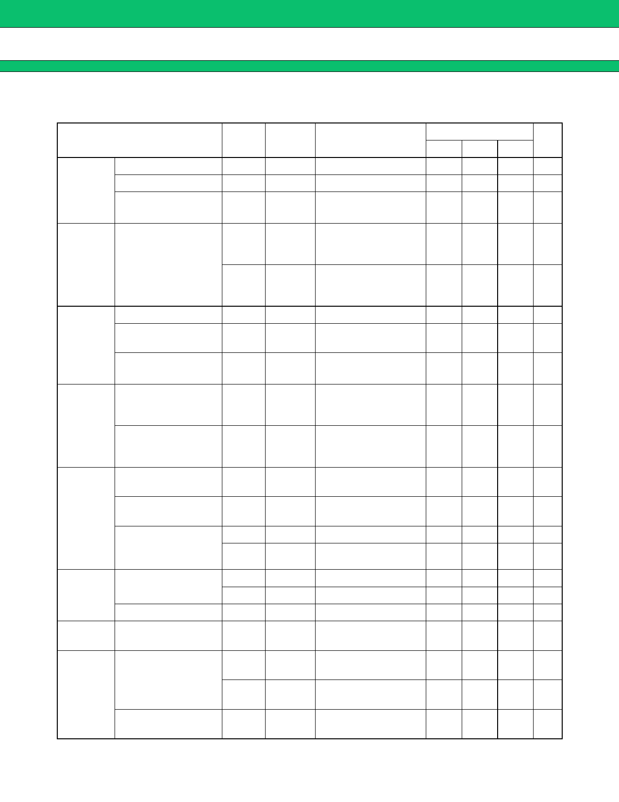
MB3825A
Parameter
Symbol
SCP
Comp.
block
(CH5,
CH6)
Input offset voltage
VIO
Input bias current
IIN+
Common mode input
voltage range
VCM
PWM
Comp.
block
(CH1 to
CH6)
Threshold voltage
VT0
VT100
Dead time
control
block
(CH3)
(DTC
terminal)
Input bias current
Sink current at
CTL2 = “L”
Input voltage
at CTL2 = “L”
IB
IIDTC
VIDTC
Main side Output source current IO−
output
block (CH1
to CH6)
(Drive-1) Output sink current
IO+
Synchro-
nous
Output source current
IO−
rectifier
side output Output sink current
IO+
block
(CH1,
VOH
CH4)
Output voltage
(Drive-2)
VOL
Control
block
CTL input condition
Input current
VON
VOFF
ICTL
VCC Comp.
block
Threshold voltage
VTH
General
Standby current
ICCS
ICCS (O)
Power supply current
ICC
Pin No
64, 4
14, 9
64, 4
46, 50,
56, 57,
64, 4
46, 50,
56, 57,
64, 4
31
31
31
46, 50,
56, 57,
64, 4
46, 50,
56, 57,
64, 4
43, 60
43, 60
43, 60
43, 60
27
27
30
46, 50,
56
28
42, 51,
63
28, 42,
51, 63
(VCC = VCC (O) = +6 V, Ta = +25°C)
Conditions
Value
Unit
Min Typ Max
0.55 0.60 0.65 V
IN (C) = 0 V
−400 −40 nA
0
VCC −
0.9
V
Duty cycle = 0%
0.55 0.65 V
Duty cycle = 100%
DTC = 0.4 V
DTC = 1.5 V
CTL2 = 0 V
IDTC = 40 µA
CTL2 = 0 V
Duty cycle ≤ 5%
1.35 1.45 V
−1.0 −0.2 µA
80 500 µA
0.2 0.3 V
−100 mA
RB = 5.6 kΩ
Duty cycle ≤ 5%,
VO = 2 V
Duty cycle ≤ 5%,
VO = 1 V
IC active mode
IC standby mode
CTL = 5 V
VCC terminal,
CTL = 0 V
VCC (O) terminal,
CTL = 0 V
7
10 13 mA
−70 mA
70 mA
3.5 4.0 V
0 0.1 V
2.1 12 V
0
0.7 V
100 200 µA
VCC − VCC − VCC −
0.70 0.65 0.60
V
10 µA
10 µA
6.3 9.0 mA
* : Standard design value.
13
Share Link: 