IS62LV12816LL-10B(2000_11) データシートの表示(PDF) - Integrated Silicon Solution
部品番号
コンポーネント説明
メーカー
IS62LV12816LL-10B Datasheet PDF : 10 Pages
| |||
IS62LV12816L/LL
ISSI ®
AC TEST CONDITIONS
Parameter
Input Pulse Level
Input Rise and Fall Times
Input and Output Timing
and Reference Level
Output Load
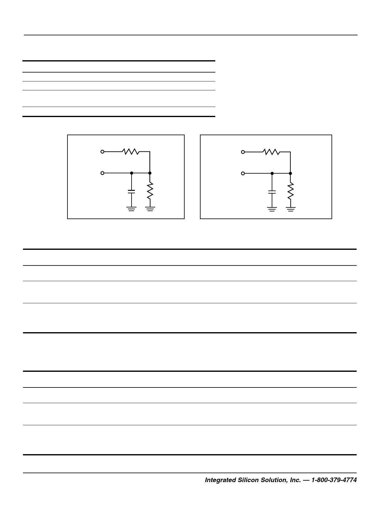
AC TEST LOADS
2.8V
Unit
0.4V to 2.2V
5 ns
1.3V
See Figures 1 and 2
3070 Ω
2.8V
3070 Ω
OUTPUT
OUTPUT
100 pF
Including
jig and
scope
3150 Ω
5 pF
Including
jig and
scope
3150 Ω
Figure 1
Figure 2
IS62LV12816L POWER SUPPLY CHARACTERISTICS(1) (Over Operating Range)
Symbol Parameter
ICC
Vcc Dynamic Operating
Supply Current
ISB1
TTL Standby Current
(TTL Inputs)
ISB2
CMOS Standby
Current (CMOS Inputs)
Test Conditions
VCC = Max.,
IOUT = 0 mA, f = fMAX
VCC = Max.,
VIN = VIH or VIL
CE ≥ VIH , f = 0
VCC = Max.,
CE ≥ VCC – 0.2V,
VIN ≥ VCC – 0.2V, or
VIN ≤ 0.2V, f = 0
Com.
Ind.
Com.
Ind.
Com.
Ind.
-55
-70
-100
Min. Max. Min. Max. Min. Max. Unit
— 40
— 60
— 30
— 50
— 20 mA
— 40
— 0.4
— 1.0
— 0.4
— 1.0
— 0.4 mA
— 1.0
— 15
— 15
— 15
µA
— 15
— 15
— 15
Note:
1. At f = fMAX, address and data inputs are cycling at the maximum frequency, f = 0 means no input lines change.
IS62LV12816LL POWER SUPPLY CHARACTERISTICS(1) (Over Operating Range)
Symbol Parameter
ICC
Vcc Dynamic Operating
Supply Current
ISB1 TTL Standby Current
(TTL Inputs)
ISB2
CMOS Standby
Current (CMOS Inputs)
Test Conditions
VCC = Max.,
IOUT = 0 mA, f = fMAX
VCC = Max.,
VIN = VIH or VIL
CE ≥ VIH , f = 0
VCC = Max.,
CE ≥ VCC – 0.2V,
VIN ≥ VCC – 0.2V, or
VIN ≤ 0.2V, f = 0
Com.
Ind.
Com.
Ind.
Com.
Ind.
-55
-70
-100
Min. Max. Min. Max. Min. Max. Unit
— 40
— 60
— 30
— 50
— 20 mA
— 40
— 0.4
— 1.0
— 0.4
— 1.0
— 0.4 mA
— 1.0
—5
—5
—5
µA
—5
—5
—5
Note:
1. At f = fMAX, address and data inputs are cycling at the maximum frequency, f = 0 means no input lines change.
4
Integrated Silicon Solution, Inc. — 1-800-379-4774
Rev. C
03/17/00
Share Link: 