ISL6558EVAL2 データシートの表示(PDF) - Renesas Electronics
部品番号
コンポーネント説明
メーカー
ISL6558EVAL2 Datasheet PDF : 10 Pages
| |||
ISL6605
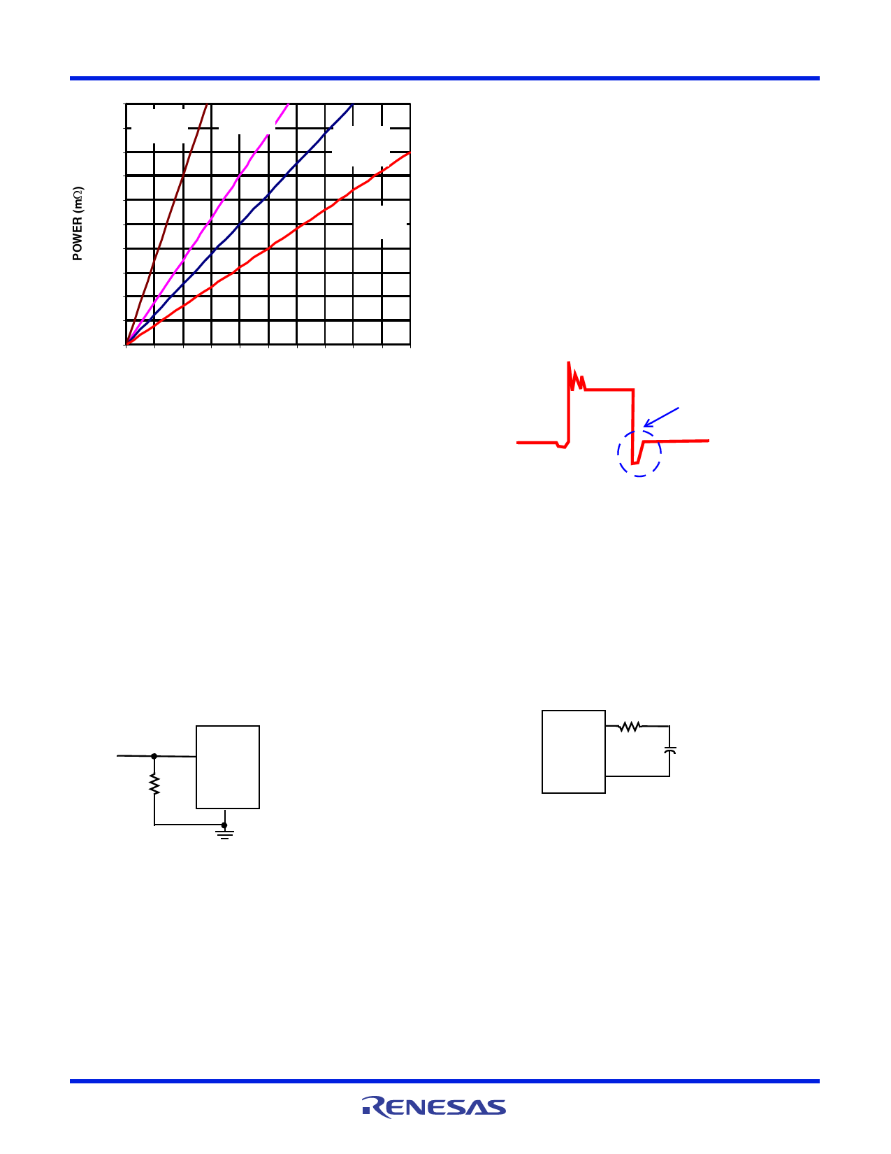
1000
900
800
700
QU=100nC
QL=200nC
QU=50nC
QL=100nC
QU=50nC
QL=50nC
600
500
QU=20nC
QL=50nC
400
300
200
100
0
0 200 400 600 800 1000 1200 1400 1600 1800 2000
FREQUENCY (KHZ)
FIGURE 2. POWER DISSIPATION VS. FREQUENCY
checked at the worst case (maximum VCC and prior to
overcurrent trip point), especially for applications with higher
than 20A per D2PAK FET. MOSFETs with low parasitic lead
inductances, such as multi-SOURCE leads devices (SO-8 and
LFPAK), are recommended.
Careful layout would help reduce the negative ringing peak
significantly:
- Tie the SOURCE of the upper FET and the DRAIN of the
lower FET as close as possible;
- Use the shortest low-impedance trace between the
SOURCE of the lower FET and the power ground;
- Tie the GND of the ISL6605 closely to the SOURCE of the
lower FET.
PHASE
Negative Spike
Application Information
Fault Mode at Repetitive Startups
At a low VCC (<2V), the Thevenin equivalent of the 20k divider
at the PWM pin, as shown in the Block Diagram on page 2, is
no longer true; very high impedance will be seen from the
PWM pin to GND. Junction leakage currents from the VCC to
the resistor tub will tend to pull up the PWM input and falsely
trigger the UGATE. If the energy stored in the bootstrap
capacitor is not completely discharged during the previous
power-down period, then the upper MOSFET could be turned
on and generate a spike at the output when VCC ramps up. A
499k resistor at the PWM to GND, as shown in Figure 3,
helps bleed the leakage currents, thus eliminating the startup
spike.
PWM
499K
ISL6605
GND
FIGURE 3. 499k RESISTOR
Layout Considerations and MOSFET Selection
The parasitic inductances of the PCB and the power devices
(both upper and lower FETs) generate a negative ringing at the
trailing edge of the PHASE node. This negative ringing plus the
VCC adds charges to the bootstrap capacitor through the
internal bootstrap schottky diode when the PHASE node is
low. If the negative spikes are too large, especially at high
current applications with a poor layout, the voltage on the
bootstrap capacitor could exceed the VCC and the device’s
maximum rating. The VBOOT-PHASE voltage should be
FIGURE 4. TYPICAL PHASE NODE VOLTAGE WAVEFORM
A resistor placement of RBOOT, as shown in Figure 5, in the
earlier design is recommended; it helps eliminate the
overcharge of the BOOT capacitor, in terms of voltage stress
across the BOOT to PHASE. When needed, 1 to 2 Ohm
RBOOT is sufficient and has little impact on the overall
efficiency. However, a design with good layout and using
MOSFETs with low parasitic lead inductances, such as multi-
SOURCE leads devices (SO-8 and LFPAK), is generally not
required such a resistor.
BOOT
ISL6605
PHASE
RBOOT
CBOOT
FIGURE 5. RESISTOR PLACEMENT FOR THE RBOOT
When placing the QFN part on the board, no vias or trace
should be running in between pin numbers 1 and 8 since a
small piece of copper is underneath the corner for the
orientation. In addition, connecting the thermal pad of the QFN
part to the power ground with a via, or placing a low noise
copper plane underneath the SOIC part is strongly
recommended for high switching frequency, high current
applications. This is for heat spreading and allows the part to
achieve its full thermal potential.
FN9091 Rev 7.00
May 9, 2006
Page 7 of 10
Share Link: 