BR24G04FJ-3A データシートの表示(PDF) - ROHM Semiconductor
部品番号
コンポーネント説明
メーカー
BR24G04FJ-3A Datasheet PDF : 36 Pages
| |||
BR24G04-3A
○ Notes on write cycle continuous input
The maximum page numbers of BR24G04-3A are 16 bytes. Any bytes below these can be written.
1 page=16bytes, but the page write cycle time is 5ms at maximum for 16byte bulk write.
It does not stand 5ms at maximum × 16byte=80ms(Max.)
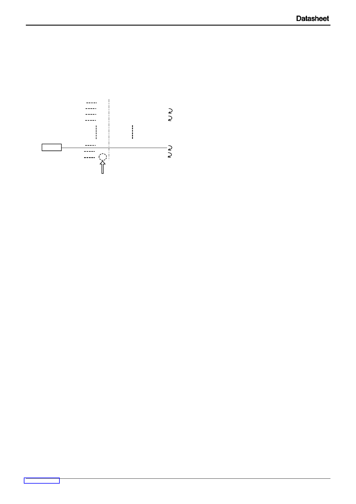
○ Internal address increment
Page write mode
WA7
WA4 WA3 WA2 WA1 WA0
0
00000
0
00001
0
00010
Increment
0Eh
0
0
0
01110
01111
00000
For example, when it is started from address 0Eh,
therefore, increment is made as below,
0Eh→0Fh→00h→01h・・・ which please note.
Significant bit is fixed.
No digit up
※0Eh・・・0E in hexadecimal, therefore, 00001110 becomes a
binary number.
○ Write protect (WP) terminal
・Write protect (WP) function
When WP terminal is set Vcc (H level), data rewrite of all addresses is prohibited. When it is set GND (L level), data
rewrite of all address is enabled. Be sure to connect this terminal to Vcc or GND, or control it to H level or L level. Do not
use it open.
In the case of use it as an ROM, it is recommended to connect it to pull up or Vcc.
At extremely low voltage at power ON / OFF, by setting the WP terminal 'H', mistake write can be prevented.
www.rohm.com
© 2014 ROHM Co., Ltd. All rights reserved.
TSZ22111 • 15 • 001
16/33
TSZ02201-0R2R0G100560-1-2
11.Jun.2019 Rev.004
Share Link: 