MJE5740 データシートの表示(PDF) - ON Semiconductor
部品番号
コンポーネント説明
メーカー
MJE5740 Datasheet PDF : 6 Pages
| |||
MJE5740, MJE5742
MJE5742 is a Preferred Device
NPN Silicon Power
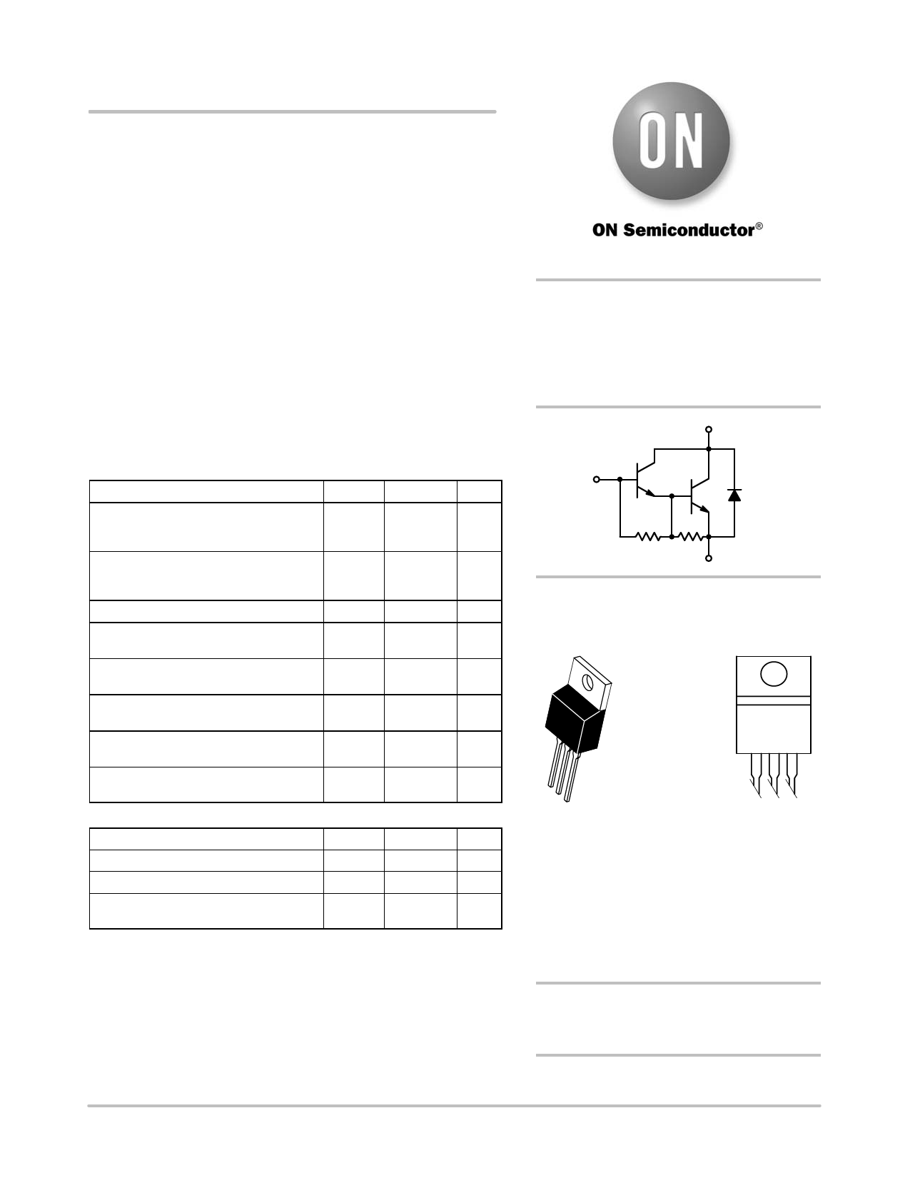
Darlington Transistors
The MJE5740 and MJE5742 Darlington transistors are designed for
high−voltage power switching in inductive circuits.
Features
• Pb−Free Packages are Available*
Applications
• Small Engine Ignition
• Switching Regulators
• Inverters
• Solenoid and Relay Drivers
• Motor Controls
http://onsemi.com
POWER DARLINGTON
TRANSISTORS
8 AMPERES
300−400 VOLTS
80 WATTS
MAXIMUM RATINGS
Rating
Collector−Emitter Voltage
Symbol
VCEO(sus)
MJE5740
MJE5742
Value
300
400
Unit
Vdc
Collector−Emitter Voltage
MJE5740
MJE5742
VCEV
Vdc
600
800
Emitter−Base Voltage
VEB
Collector Current − Continuous
IC
− Peak (Note 1)
ICM
Base Current
− Continuous
IB
− Peak (Note 1)
IBM
Total Device Dissipation @ TC = 25_C
PD
Derate above 25°C
8
Vdc
8
Adc
16
2.5
Adc
5
2
W
16
W/_C
Total Device Dissipation @ TC = 25_C
PD
Derate above 25°C
80
W
640
W/_C
Operating and Storage Junction
Temperature Range
TJ, Tstg −65 to +150 _C
THERMAL CHARACTERISTICS
Characteristics
Symbol
Max
Unit
Thermal Resistance, Junction−to−Case
RqJC
1.25
_C/W
Thermal Resistance, Junction−to−Ambient RqJA
62.5
_C/W
Maximum Lead Temperature for Soldering
TL
Purposes 1/8″ from Case for 5 Seconds
275
_C
Maximum ratings are those values beyond which device damage can occur.
Maximum ratings applied to the device are individual stress limit values (not
normal operating conditions) and are not valid simultaneously. If these limits are
exceeded, device functional operation is not implied, damage may occur and
reliability may be affected.
1. Pulse Test: Pulse Width = 5 ms, Duty Cycle ≤ 10%.
*For additional information on our Pb−Free strategy and soldering details, please
download the ON Semiconductor Soldering and Mounting Techniques
Reference Manual, SOLDERRM/D.
© Semiconductor Components Industries, LLC, 2006
1
February, 2006 − Rev. 6
≈ 100 ≈ 50
MARKING
DIAGRAM
123
TO−220AB
CASE 221A−09
STYLE 1
MJE574xG
AY WW
MJE574x
G
A
Y
WW
= Device Code
x = 0 or 2
= Pb−Free Package
= Assembly Location
= Year
= Work Week
ORDERING INFORMATION
See detailed ordering and shipping information in the package
dimensions section on page 2 of this data sheet.
Preferred devices are recommended choices for future use
and best overall value.
Publication Order Number:
MJE5740/D
Share Link: 