BUL45 データシートの表示(PDF) - Motorola => Freescale
部品番号
コンポーネント説明
メーカー
BUL45 Datasheet PDF : 10 Pages
| |||
BUL45 BUL45F
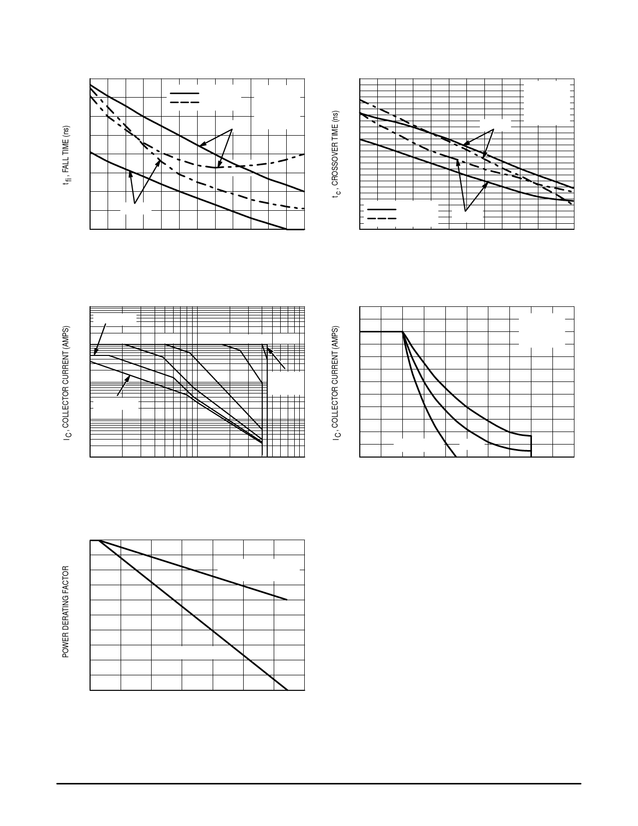
TYPICAL SWITCHING CHARACTERISTICS
(IB2 = IC/2 for all switching)
150
300
140
130
TJ = 25°C
IB(off) = IC/2
TJ = 125°C
VCC = 15 V
VZ = 300 V
250
IC = 1 A LC = 200 µH
120
200
110
100
150
IC = 1 A
VCC = 15 V
VZ = 300 V
IB(off) = IC/2
LC = 200 µH
90
80
IC = 2 A
70
3 4 5 6 7 8 9 10 11 12 13 14 15
hFE, FORCED GAIN
100
TJ = 25°C
TJ = 125°C
IC = 2 A
50
3 4 5 6 7 8 9 10 11 12 13 14 15
hFE, FORCED GAIN
Figure 13. Inductive Fall Time, tfi(hFE)
Figure 14. Crossover Time
100
DC (BUL45)
5 ms
10
GUARANTEED SAFE OPERATING AREA INFORMATION
6
5
1 ms
50 µs 10 µs 1 µs
4
TC ≤ 125°C
IC/IB ≥ 4
LC = 500 µH
1.0
DC (BUL45F)
0.1
EXTENDED
SOA
0.01
10
100
1000
VCE, COLLECTOR–EMITTER VOLTAGE (VOLTS)
Figure 15. Forward Bias Safe Operating Area
3
2
–5 V
1
VBE(off) = 0 V
–1.5 V
0
300
400
500
600
700
800
VCE, COLLECTOR–EMITTER VOLTAGE (VOLTS)
Figure 16. Reverse Bias Switching Safe Operating Area
1.0
0.8
SECOND BREAKDOWN
DERATING
0.6
0.4
THERMAL DERATING
0.2
0
20
40
60
80 100 120 140 160
TC, CASE TEMPERATURE (°C)
Figure 17. Forward Bias Power Derating
There are two limitations on the power handling ability of a
transistor: average junction temperature and second break-
down. Safe operating area curves indicate IC – VCE limits of
the transistor that must be observed for reliable operation;
i.e., the transistor must not be subjected to greater dissipation
than the curves indicate. The data of Figure 15 is based on TC
= 25°C; TJ(pk) is variable depending on power level. Second
breakdown pulse limits are valid for duty cycles to 10% but
must be derated when TC ≥ 25°C. Second breakdown limita-
tions do not derate the same as thermal limitations. Allowable
current at the voltages shown in Figure 15 may be found at
any case temperature by using the appropriate curve on Fig-
ure 17. TJ(pk) may be calculated from the data in Figures 20
and 21. At any case temperatures, thermal limitations will re-
duce the power that can be handled to values less than the
limitations imposed by second breakdown. For inductive
loads, high voltage and current must be sustained simulta-
neously during turn–off with the base–to–emitter junction re-
verse–biased. The safe level is specified as a reverse–biased
safe operating area (Figure 16). This rating is verified under
clamped conditions so that the device is never subjected to
an avalanche mode.
Motorola Bipolar Power Transistor Device Data
5
Share Link: 